Metal-semiconductor electrode structure and preparation method thereof

An electrode structure and metal electrode technology, which is applied in the manufacture of semiconductor/solid-state devices, semiconductor devices, circuits, etc., can solve the problems of annealing and other processes that are inevitable, contact metals cannot be found, and the preparation process is complicated, so as to improve the energy band state, Low cost and good reproducibility

Inactive Publication Date: 2011-05-18
SUZHOU NANOWIN SCI & TECH +1
View PDF4 Cites 38 Cited by
  • Summary
  • Abstract
  • Description
  • Claims
  • Application Information

AI Technical Summary

Problems solved by technology

[0006] At present, although the ohmic contact research of n-type semiconductors with metal (alloy) as the electrode is relatively systematic and in-depth, and the contact resistivity can reach 10 -5 ~10 -8 Ωcm -2 , but the preparation process is still relatively complicated, and processes such as evaporation of multi-layer metal electro

Method used


Image

  • Metal-semiconductor electrode structure and preparation method thereof
  • Metal-semiconductor electrode structure and preparation method thereof
  • Metal-semiconductor electrode structure and preparation method thereof

Examples


Embodiment 1

[0024] Embodiment 1 is described by taking an intrinsic GaN crystal as an example of a semiconductor layer.

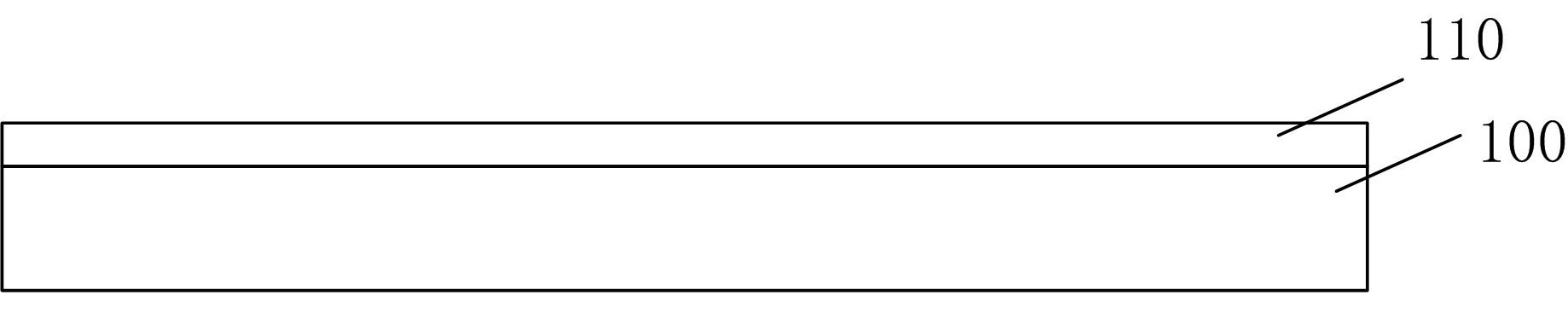
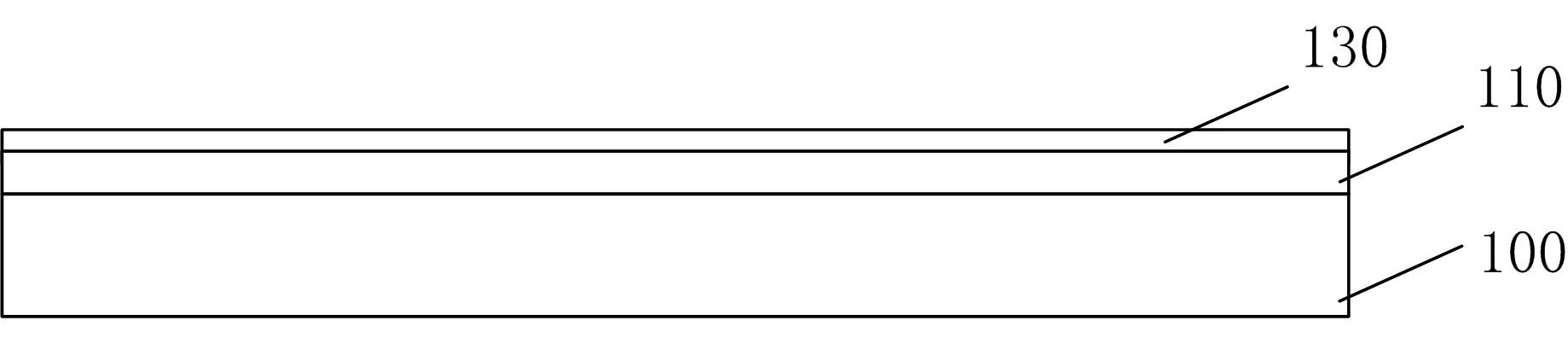
[0025] Step 11, refer to attached Figure 2A, Graphene preparation: the graphene film 110 is prepared on the surface of the growth substrate 100 by chemical vapor deposition. The specific implementation of the chemical vapor deposition method belongs to the known technology and will not be described in detail here. This step needs to provide a separate growth substrate 100 for the chemical vapor substrate process. The chemical vapor deposition process can form a graphene film on the surface of the growth substrate 100, and this process has very broad requirements on the material of the growth substrate 100. Many common substrate materials, such as single crystal silicon, sapphire, glass and even metal Substrates can meet the requirements. The graphene film 110 can also be grown by wet chemical method. The graphene film 110 is graphene without p-type or n-type doping...

Embodiment 2

[0035] Embodiment 2: It is described by taking a P-type GaN crystal as an example of a semiconductor layer.

[0036] Step 21, graphene preparation: the graphite redox method is used to prepare the graphene powder material. The specific implementation of the graphite reduction method belongs to the known technology and will not be described in detail here.

[0037] Step 22, cleaning the p-type GaN crystal: cleaning the surface with organic solvents such as acetone and alcohol.

[0038] Step 23, covering the p-type GaN crystal with a graphene layer: spin coating the graphene powder material on the p-type GaN crystal.

[0039] Step 24, evaporating metal: using a vacuum evaporation method to cover the conductive metal layer on the graphene layer.

[0040] Step 25, forming an etching stopper layer on the surface of the metal layer.

[0041] Step 26, using inductively coupled plasma (ICP) to etch the metal layer and the graphene layer until the p-type GaN crystal stops, forming a...


PUM


Abstract

The invention relates to a metal-semiconductor electrode structure which comprises a semiconductor layer and a metal electrode, and a graphene layer is further arranged between the semiconductor layer and the metal electrode to reduce the contact resistance between the metal electrode and the semiconductor layer. The metal-semiconductor electrode structure provided by the invention has the advantages of improving the energy band state of metal-semiconductor contact by inserting the graphene layer between the metal and the semiconductor layer, being widely applicable to metals with different work functions and semiconductors with different doping types and doping concentrations, and reducing the contact potential barrier, thereby playing the function of reducing the contact resistance. The metal-semiconductor electrode structure provided by the invention has simple preparation method, stable performance, good repeatability and low cost and plays an important role in realizing micro nano semiconductor electronic devices with high performance and low cost.

Description

technical field [0001] The invention relates to the technical field of semiconductor devices and processes, in particular to a metal-semiconductor electrode structure and a preparation method thereof. Background technique [0002] An important process in the research of semiconductor devices is to use metals or alloys to make low-resistance contact electrodes. As we all know, the traditional semiconductor contact electrode production needs to process the semiconductor surface with chemical solvents, then sputter the metal film, and then perform annealing and other processes. Natural oxide layers on the sample surface and device process contamination can also significantly degrade contact characteristics. In addition, deep level traps also have a trapping effect on carriers. These factors increase the fabrication difficulty and contact characteristics of the contact electrodes. [0003] Contact electrodes on semiconductors are generally divided into two categories, namely ...

Claims


Application Information

Patent Timeline
IPC IPC(8): H01L29/47H01L21/28H01L21/285
Inventor 钟海舰刘争晖徐耿钊蔡德敏张学敏刘立伟樊英民王建峰
Owner SUZHOU NANOWIN SCI & TECH
Why Eureka
Try Eureka