Cantilever trace detection sensor and preparation method thereof
A detection sensor and cantilever beam technology, applied in the field of cantilever beam trace detection sensors and their preparation, can solve the problems of cantilever beam sensitivity limitation and the like
- Summary
- Abstract
- Description
- Claims
- Application Information
AI Technical Summary
Problems solved by technology
Method used
Image
Examples
Embodiment 1
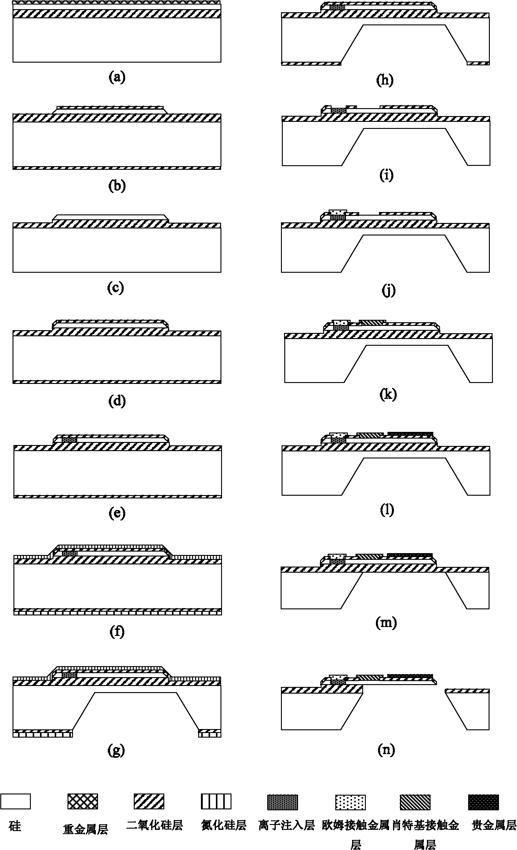
[0102] Example 1. Metal-silicon Schottky diode-embedded cantilever beams diffused by heavy metals prepared by using KOH solution to corrode the back cavity
[0103] figure 2 It is a flow chart for the preparation of the cantilever beam sensor of the present invention, and the specific steps are as follows:
[0104] 1) On the silicon device layer of the SOI sheet, use the magnetron sputtering method (atmospheric pressure is 1mTorr, current density is 10mA / cm 2 , the power density is 20W / cm 2 ) to prepare a layer of gold metal layer with a thickness of 8nm (such as figure 2 a), then utilize the high temperature diffusion method (the temperature is 350 ℃, the time is 30min) to make the metal in the metal layer diffuse into the silicon device layer, use 4g KI, 1g I 2 and 40mL H 2 The etching solution composed of O corrodes the remaining metal on the surface of the silicon device layer;
[0105] In this step, the SOI sheet is supported by a silicon device layer with a thickn...
Embodiment 2
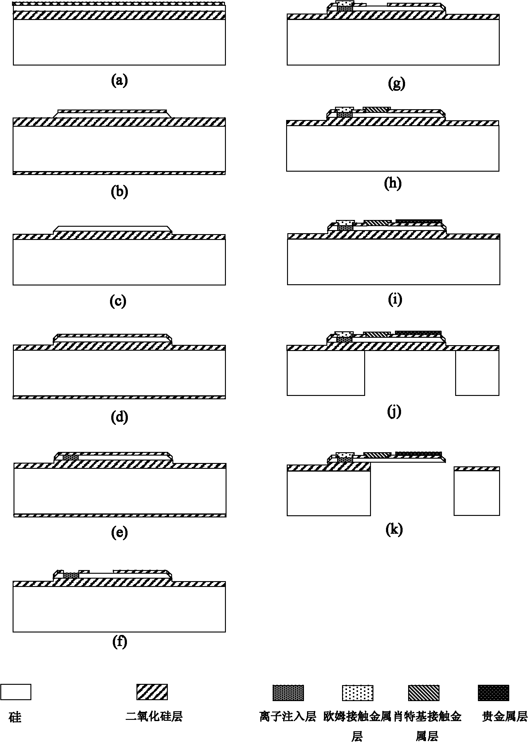
[0120] Example 2. Fabrication of metal-silicon Schottky diode-embedded cantilever beams diffused by heavy metals using ICP dry etching back cavity process
[0121] image 3 It is a flow chart for the preparation of the cantilever beam sensor of the present invention, and the specific steps are as follows:
[0122] 1) On the silicon device layer of the SOI sheet, use the magnetron sputtering method (atmospheric pressure is 1mTorr, current density is 10mA / cm 2 , the power density is 20W / cm 2 ) to prepare a layer of gold metal layer with a thickness of 8nm (such as image 3 a), then utilize the high temperature diffusion method (the temperature is 350 ℃, the time is 30min) to make the metal in the metal layer diffuse into the silicon device layer, use 4g KI, 1g I 2 and 40mL H 2 The etching solution composed of O corrodes the remaining metal on the surface of the silicon device layer;
[0123] Wherein, the SOI sheet is composed of a silicon device layer with a thickness of 1....
Embodiment 3
[0138] Example 3. Using the KOH solution to etch the back cavity process to prepare a metal-silicon Schottky diode embedded cantilever beam and irradiate it with gamma rays
[0139] Figure 4 It is a flow chart for the preparation of the cantilever beam sensor of the present invention, and the specific steps are as follows:
[0140] 1) On SOI slices (such as Figure 4 a) The silicon dioxide layer B with a thickness of 100nm is prepared by wet oxygen oxidation (oxidation temperature: 900°C) on both the front and back sides of the silicon device layer, and then patterned, using the silicon dioxide layer B as a mask Etch the silicon device layer until the silicon dioxide layer is exposed (eg Figure 4 b), then corrode the silicon dioxide layer B as a mask with an etching solution composed of hydrofluoric acid and ammonium fluoride with a volume ratio of 1:4 (such as Figure 4 c);
[0141] Wherein, the SOI sheet is composed of a silicon device layer with a thickness of 1.5 μm,...
PUM
| Property | Measurement | Unit |
|---|---|---|
| thickness | aaaaa | aaaaa |
| thickness | aaaaa | aaaaa |
| thickness | aaaaa | aaaaa |
Abstract
Description
Claims
Application Information


