Method for manufacturing semiconductor device

A manufacturing method and semiconductor technology, applied in the fields of semiconductor devices, semiconductor/solid-state device manufacturing, electrical components, etc., can solve the problems of large performance differences of semiconductor devices and reduced performance of semiconductor devices, and achieve the effect of reducing performance differences and improving performance.

Inactive Publication Date: 2011-06-15
SEMICON MFG INT (SHANGHAI) CORP +1
View PDF5 Cites 13 Cited by
  • Summary
  • Abstract
  • Description
  • Claims
  • Application Information

AI Technical Summary

Problems solved by technology

[0041] However, in the above step 108, after the polysilicon gates of the NMOS transistor and the PMOS transistor are removed, the barrier layer under the polysilicon gate is exposed to the air, because the composition of the barrier layer is titanium nitride, and titanium nitride is easily Oxygen in the air is oxidized, and titanium nitride will shrink after being oxidized. When the work function gate metal and metal aluminum are deposited on the titanium nitride to form a metal gate, the bottom width of the metal gate is smaller than the upper width. , thereby reducing the performance of the semiconductor device. Furthermore, due to the difference between the bottom width and the upper width of the metal gate, it is difficult to precisely control the width of the metal gate of the semiconductor device, which may cause the semiconductor device The performance difference is relatively large

Method used


Image

  • Method for manufacturing semiconductor device
  • Method for manufacturing semiconductor device
  • Method for manufacturing semiconductor device

Examples


Embodiment Construction

[0063] In order to make the object, technical solution and advantages of the present invention clearer, the solutions of the present invention will be further described in detail below with reference to the accompanying drawings and examples.

[0064] Figure 13 It is a flowchart of a manufacturing method of a semiconductor device provided by the present invention. Such as Figure 13 As shown, the method includes the following steps:

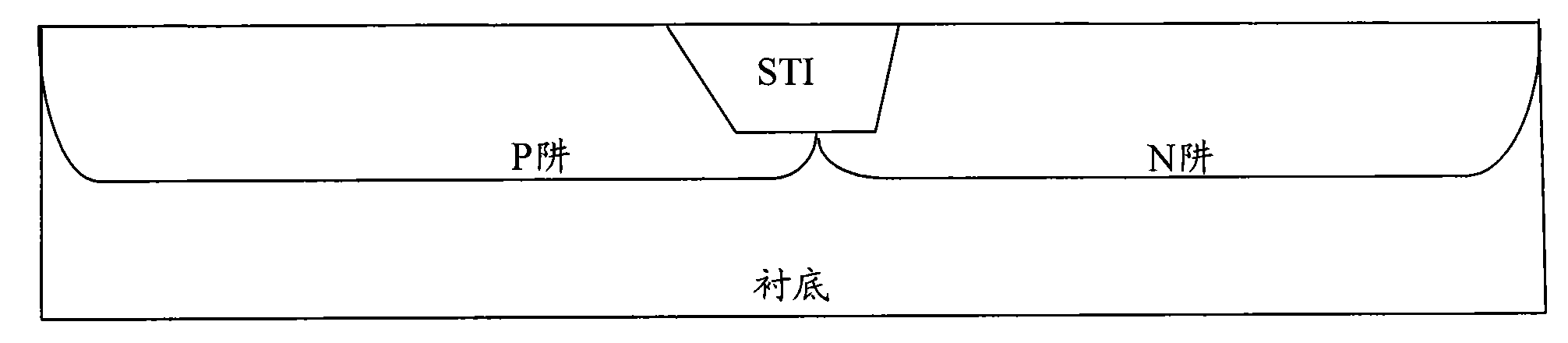
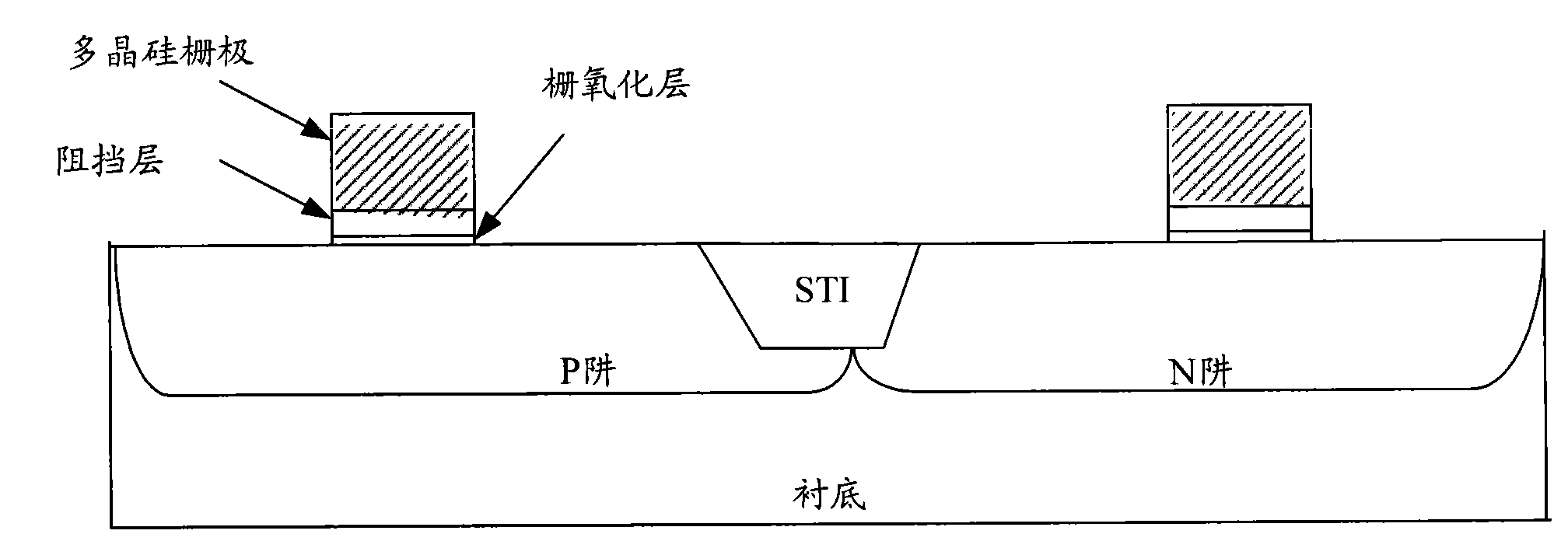
[0065] In step 201, an STI for isolating the active region is formed in the substrate, and a high dielectric constant gate oxide layer, a titanium nitride barrier layer and After the temporary polysilicon gate, auxiliary sidewall layers on both sides of the temporary polysilicon gate of the NMOS transistor and the PMOS transistor are formed.

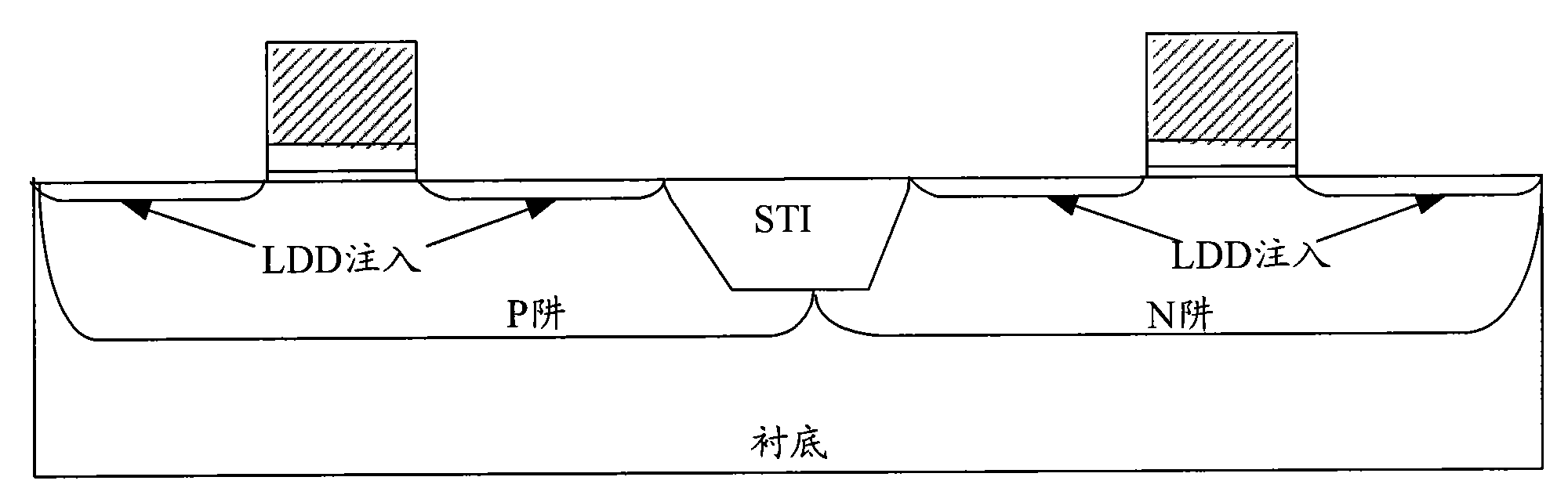
[0066] Step 202 , perform LDD implantation on the substrate on both sides of the temporary polysilicon gates of the NMOS transistor and the PMOS transistor.

[0067] Step 203 , forming sidewall layers ...


PUM

PropertyMeasurementUnit
thicknessaaaaaaaaaa

Abstract

The invention discloses a method for manufacturing a semiconductor device, which comprises the following steps of: forming a shallow trench isolation region for isolating an active region in a substrate; forming a high dielectric constant grid oxide layer, a titanium nitride blocking layer and a temporary polycrystalline silicon grid, sequentially positioned on the substrate, of an N-type metal oxide semiconductor (NMOS) tube and a P-type metal oxide semiconductor (PMOS) tube in the active region respectively; and then forming auxiliary side wall layers on two sides of the temporary polycrystalline silicon grids of the NMOS tube and the PMOS tube. The method can improve the performance of the semiconductor device and reduce the performance difference between the semiconductor devices at the same time.

Description

technical field [0001] The invention relates to semiconductor technology, in particular to a manufacturing method of a semiconductor device. Background technique [0002] In order to control the short channel effect, smaller device size further requires increased gate capacitance. This can be achieved by continuously reducing the thickness of the gate oxide layer, but with the attendant increase of gate leakage current. Especially when silicon dioxide is used as the gate oxide layer and the thickness is less than 1 nanometer, the leakage current becomes unbearable. An effective way to solve the above problems is to replace silicon dioxide with high dielectric constant insulating materials. High dielectric constant insulating materials can be hafnium silicate, hafnium silicon oxynitride, hafnium oxide, etc., and the dielectric constant is generally greater than 15. , the use of this material can further increase the gate capacitance, and at the same time the gate leakage cu...

Claims


Application Information

Patent Timeline
Patent Type & Authority Applications(China)
IPC IPC(8): H01L21/8238H01L21/28
Inventor 宁先捷
Owner SEMICON MFG INT (SHANGHAI) CORP
Why Eureka
Try Eureka