Integrated double longitudinal channel SOI LDMOS (silicon on insulator laterally double diffusion metal oxide semiconductor) device unit

A vertical and device technology, applied in the field of microelectronics, can solve the problems that are not conducive to improving the reliability of devices and systems, saving energy and protecting the environment, low working efficiency of devices, large on-state resistance of devices, etc., to achieve extended conductive current path, Effect of reducing on-state resistance and on-state voltage drop and eliminating peak electric field

Inactive Publication Date: 2011-06-15
SERVICE CENT OF COMMLIZATION OF RES FINDINGS HAIAN COUNTY
View PDF5 Cites 2 Cited by
  • Summary
  • Abstract
  • Description
  • Claims
  • Application Information

AI Technical Summary

Problems solved by technology

When the SOI LDMOS device is turned on, its conductive channel is on the silicon side surface of the interface between the vertical gate oxide layer and the top layer semiconductor, and is a vertical channel. The pn junction reverse depletion region formed by the drift region and the well region makes the current flow in the The path of the r...

Method used


Image

  • Integrated double longitudinal channel SOI LDMOS (silicon on insulator laterally double diffusion metal oxide semiconductor) device unit
  • Integrated double longitudinal channel SOI LDMOS (silicon on insulator laterally double diffusion metal oxide semiconductor) device unit
  • Integrated double longitudinal channel SOI LDMOS (silicon on insulator laterally double diffusion metal oxide semiconductor) device unit

Examples


Embodiment Construction

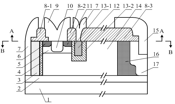
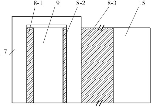
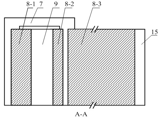
[0012] Such as figure 1 , 2 , 3 and 4, an integrated vertical double-channel SOI nLDMOS device unit includes a semiconductor substrate (1), covered with a buried oxide layer (2) on the semiconductor substrate (1), and a buried oxide layer (2) A lightly doped drift region (14) is arranged on it. One side of the lightly doped drift region (14) is set as a same-type heavily doped semiconductor region as a buffer zone (16) for LDMOS, and the other side is set with an N-type heavily doped first low-resistance polysilicon gate (3) A vertical gate oxide layer (4) is arranged between the first low-resistance polysilicon gate (3) and the lightly doped drift region (14).

[0013] A well region (5) and a groove oxygen region are arranged on the top of the lightly doped drift region (14), the well region (5) is an anisotropic heavily doped semiconductor region, the groove oxygen region is an oxide layer, and one part of the well region (5) One side is arranged adjacent to the vertical ...


PUM


Abstract

The invention relates to an integrated double longitudinal channel SOI LDMOS (silicon on insulator laterally double diffusion metal oxide semiconductor) device unit. Improvement on the device structure and electrical properties of the traditional product is restricted. In the invention, a hidden buried oxidation layer divides a semiconductor substrate into a semiconductor substrate and a lightly doped drift region, wherein the two sides of the lightly doped drift region are respectively provided with a buffer zone of the LDMOS and a first low resistance polycrystalline silicon gate, and a longitudinal gate oxidation layer is arranged between the first low resistance polycrystalline silicon gate and the lightly doped drift region. The top of the lightly doped drift region is provided with a well region and a slot oxygen region, the well region is internally provided with two source electrodes and an ohm contact region, and the slot oxygen region is internally embedded with a second polycrystalline silicon gate. The upper part of the device is provided with three field oxidation layers and a metal layer. In the invention, a shallow slot gate is added between the well region and the drift region, a longitudinal conducting channel is added, the transconductance and on state current of the device are improved, and the on state resistance and on state voltage drop of the device are reduced, thus the on state power consumption is reduced, the thermostability and resistance to voltage of the device are improved, and the reliability of the device is improved.

Description

technical field [0001] The invention belongs to the technical field of microelectronics and relates to an integrated double vertical channel (DVC) SOI (semiconductor on insulating layer) LDMOS (lateral double injection metal-oxide-semiconductor field effect transistor) device unit. Background technique [0002] Due to its high integration, high operating frequency and temperature, strong radiation resistance, minimal parasitic effects, low cost and high reliability, SOI LDMOS devices are used as contactless high frequency Power electronic switches or power amplifiers and drivers are widely used in the fields of intelligent power electronics, high-temperature environment power electronics, space power electronics, vehicle power electronics, and radio frequency communications. Integrated Vertical Channel SOI nLDMOS is nLDMOS on SOI substrate - A field oxide layer is formed on the top layer semiconductor; a deep groove is etched near the source side and a vertical thin gate ox...

Claims


Application Information

Patent Timeline
IPC IPC(8): H01L29/78H01L29/06H01L21/762H01L21/768
Inventor 张海鹏许生根陈波李浩
Owner SERVICE CENT OF COMMLIZATION OF RES FINDINGS HAIAN COUNTY
Why Eureka
Try Eureka