
Organic transistor and method for manufacturing the same

A technology of organic transistors and manufacturing methods, applied in the direction of transistors, semiconductor/solid-state device manufacturing, electric solid-state devices, etc., can solve problems such as unpredictable transistor component performance, and achieve high alignment and crystallinity, high effect, and excellent transistors The effect of the characteristic

Active Publication Date: 2013-04-03
DIC CORP
View PDF1 Cites 0 Cited by
  • Summary
  • Abstract
  • Description
  • Claims
  • Application Information

AI Technical Summary

Problems solved by technology

However, there is no description about adding a fluorine-based surfactant, and it is not expected that the performance of a transistor device can be improved by using an organic semiconductor to which a fluorine-based surfactant is added.

Method used


Image

  • Organic transistor and method for manufacturing the same
  • Organic transistor and method for manufacturing the same

Examples


Embodiment

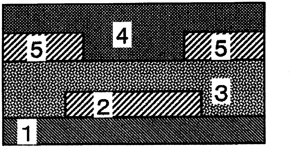
[0074] Below, create figure 1 The test element having the bottom-gate-bottom-contact (BGBC) structure shown was used for evaluating the characteristics of the organic transistor of the present invention. From the measured values ​​of Id-Vg and Id-Vd, the field-effect mobility and ON / OFF value were calculated.

Synthetic example 1

[0075] (Synthesis Example 1) Synthesis of Fluoro(meth)acrylate Polymer (1)

[0076]Into a glass flask equipped with a stirring device, a condenser, a thermometer, and a dropping funnel, 27 parts by weight of a fluorinated (meth)acrylate (A-1) and a polyamide as a non-fluorine (meth)acrylate were weighed and added. 21.6 parts by weight of propylene oxide monomethacrylate (average degree of polymerization: 5), 5.4 parts by weight of 3-methacryloxypropyltris(trimethylsiloxy)silane, 66.1 parts by weight of methyl ethyl ketone (MEK) as a polymerization solvent parts by weight, and 0.54 parts by weight of dimethyl 2,2'-azobis(2-methylpropionate) as a polymerization initiator. In addition, 63 parts by weight of (A-1), 50.4 parts by weight of polyoxypropylene monomethacrylate (average degree of polymerization: 5), 3-methacryloyloxypropyl tris(trimethylsiloxane) and 12.6 parts by weight of silane, 124.2 parts by weight of MEK, and 1.26 parts by weight of dimethyl 2,2'-azobis(2-methylp...

Synthetic example 2

[0077] (Synthesis Example 2) Synthesis of Fluorinated (Meth)acrylate Polymer (2)

[0078] 9.3 g of (A-1) as a fluorinated (meth)acrylate and 4-(6-acryloyloxyhexyloxy)benzene as a non-fluorinated (meth)acrylate were weighed into a glass polymerization tube. 18 g of benzene, 220 ML of toluene as a polymerization solvent, 2,2' azobis(2,4-dimethylvaleronitrile) and 0.55 g of (A-1) as a polymerization initiator. After blowing nitrogen stream into this solution to remove oxygen, it was made to react at 60 degreeC for 24 hours. After completion of the reaction, the reaction liquid was concentrated, and the concentrated liquid was added dropwise to 1 L of methanol. The precipitated solid was sufficiently washed with methanol to obtain a fluorinated (meth)acrylate polymer (2). The polystyrene-equivalent weight average molecular weight of the obtained polymer (2) by GPC was Mw=47000.


PUM


Abstract

The object of the present invention is to provide an organic transistor using an organic semiconductor having excellent transistor properties, and a method for producing the organic transistor, the present invention providing, first, an organic transistor including a gate electrode (b), an insulating layer (c), an organic semiconductor layer (d) which contacts the insulating layer (c) and has a channel formation area, and source / drain electrodes (e), which are formed on (a) a substrate, wherein the organic semiconductor layer (d) contains a fluorine-based compound (surfactant), and, secondly, a method for producing an organic transistor comprising a gate electrode (b), an insulating layer (c), an organic semiconductor layer (d) which contacts the insulating layer (c) and has a channel formation area, and source / drain electrodes (e), which are formed on (a) a substrate, the method comprising: a step in which the organic semiconductor layer (d) is formed on the insulating layer (c) by printing or coating an organic semiconductor solution containing a fluorine-based surfactant; or a step in which the insulating layer (d) is formed on the organic semiconductor layer (d) containing a fluorine-based surfactant by printing or coating.

Description

technical field [0001] The present invention relates to an organic transistor using an organic semiconductor used in liquid crystal displays, electronic paper, EL display devices, RF-ID tags, and the like, and a method for manufacturing the same. Background technique [0002] Transistors are widely used as important electronic elements (electronic parts) constituting televisions and computer equipment, and are currently manufactured using inorganic substances such as silicon as main materials. In recent years, organic transistors using organic substances as components of such transistors have attracted attention (see Non-Patent Document 1). Since organic transistors can be formed by wet methods such as printing methods, there is no need for expensive vacuum devices that are necessary in the conventional silicon process, and production costs including equipment investment can be greatly reduced. In addition, the process can be lowered in temperature, and It can also be forme...

Claims


Application Information

Patent Timeline
Patent Type & Authority Patents(China)
IPC IPC(8): H01L29/786H01L21/336H01L51/05H01L51/30H01L51/40
CPCH01L51/0007H01L51/0545H01L51/0562H01L51/0558H01L51/0003H01L51/0529H01L51/0566H10K71/15H10K71/12H10K10/488H10K10/484H10K10/466
Inventor 高武正义笠井正纪米原祥友高野圣史
Owner DIC CORP
Learn More