Boron-doped diamond micro-nano material with columnar array structure and preparation method thereof

An array structure and boron doping technology, applied in the field of micro-nano materials, can solve the problems of destroying the boron-doped diamond crystal plane structure, complicated preparation process, poor integrity of the porous alumina film, etc., and achieves a simple and easy preparation process. Capture and achieve controllable effects

Active Publication Date: 2011-07-20
DALIAN UNIV OF TECH
View PDF5 Cites 26 Cited by
  • Summary
  • Abstract
  • Description
  • Claims
  • Application Information

AI Technical Summary

Problems solved by technology

[0003] At present, researchers mainly use chemical vapor deposition, combined with active ion etching technology and application template method, and assist hot wire chemical vapor deposition technology to prepare micro-nano structure and nano-structure array diamond, such as Masuda, H. et al. in Adv.Mater. (2000, 12, 444~447): "Fabrication of a Nanostructured Diamond Honeycomb Film" (preparation of honeycomb nanostructured diamond film) article, described the preparation of diamond film by chemical vapor deposition, and the preparation of general anodic oxidation method. The transparent porous alumina film is used as a mask, and the method of oxygen plasma etching is used to prepare a honeycomb diamond film with a fine diameter. The preparation process is relatively complicated, and the integrity of the porous alumina film is not strong. The crystallographic structure of boron-doped diamond may be destroyed during the etching process

Method used


Image

  • Boron-doped diamond micro-nano material with columnar array structure and preparation method thereof
  • Boron-doped diamond micro-nano material with columnar array structure and preparation method thereof
  • Boron-doped diamond micro-nano material with columnar array structure and preparation method thereof

Examples


Embodiment 1

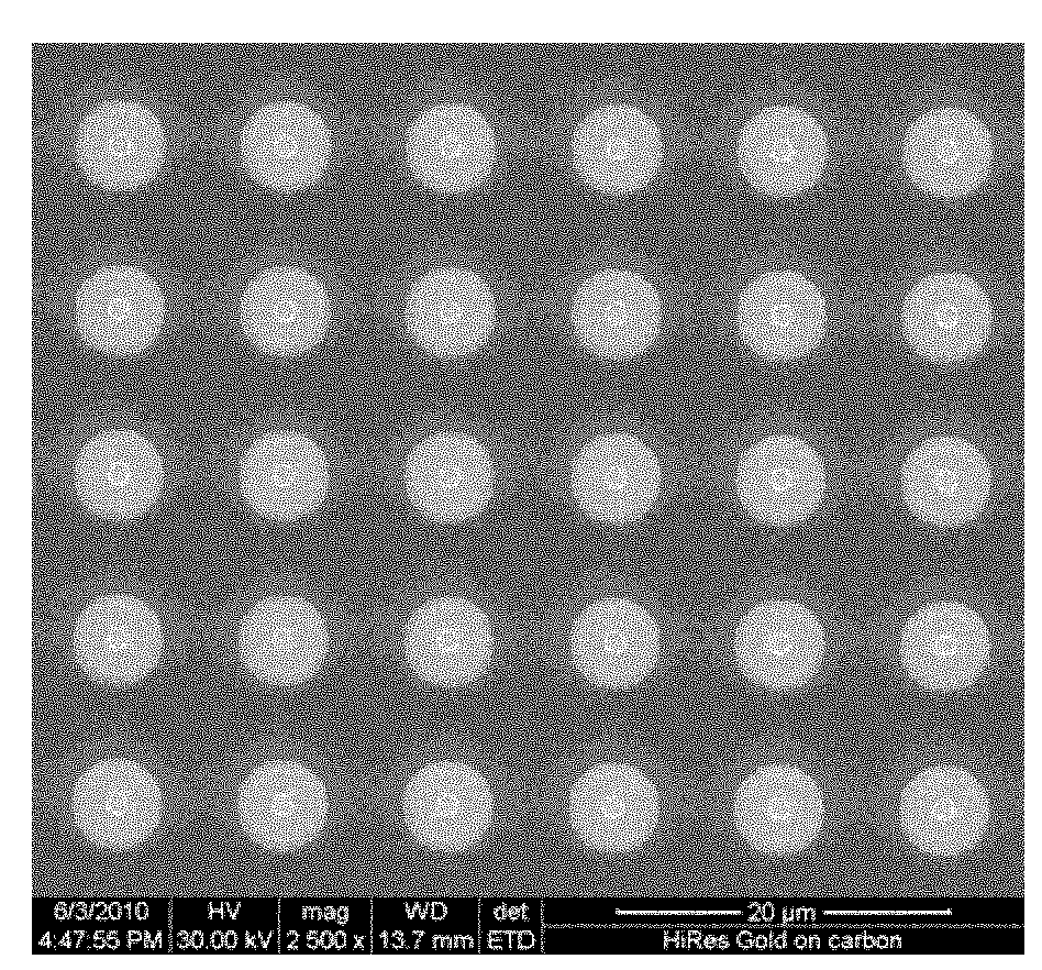
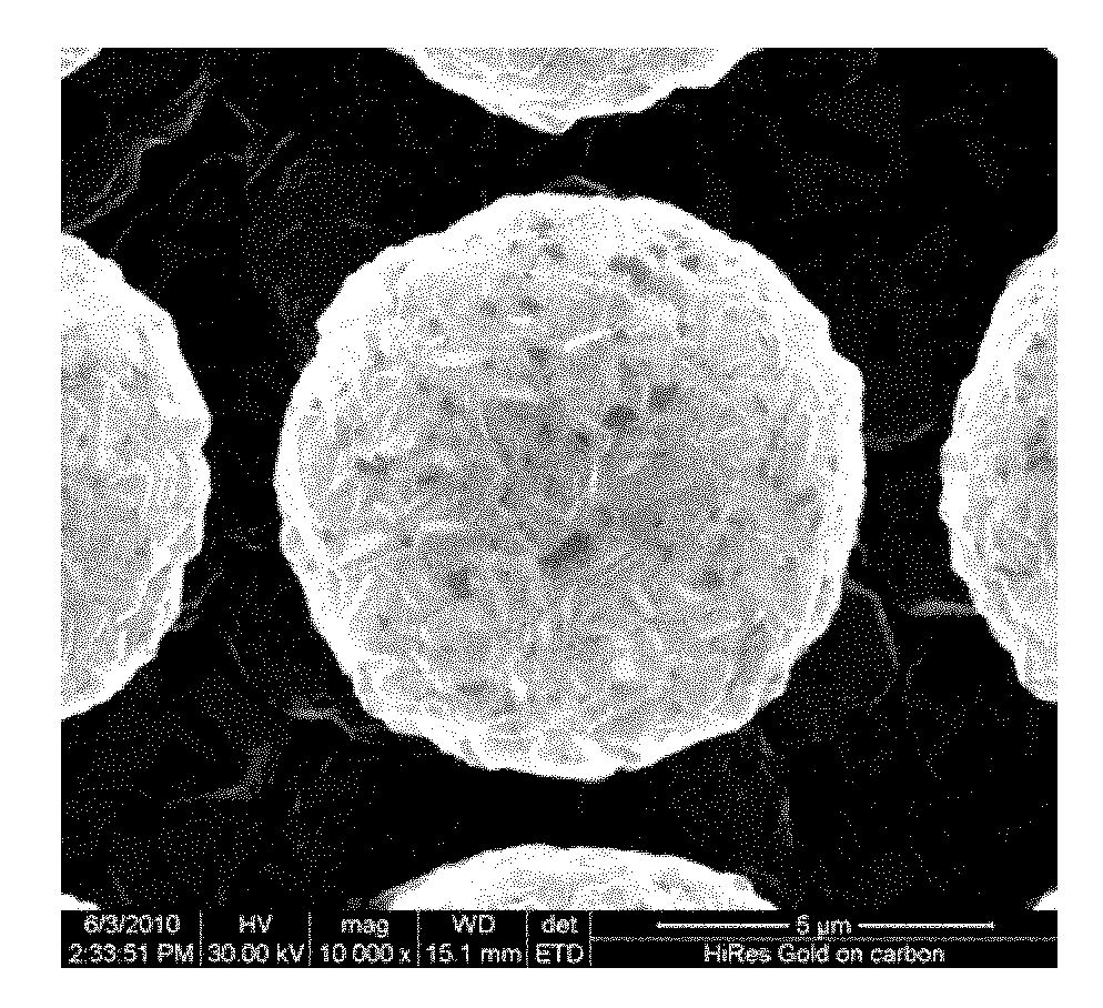
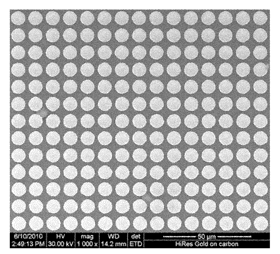
[0028] Example 1, a boron-doped diamond micro-nano material with a columnar array structure was prepared on a columnar array silicon substrate with a column height of 10 μm, a diameter of 5 μm, and a column spacing of 5 μm.

[0029] The production steps are as follows:

[0030] The first step is to select silicon with a crystal plane of (111), first oxidize the silicon surface to form an oxide layer, then spin-coat a photoresist coating on the surface of the oxide layer, expose and develop with ultraviolet light under the mask, and make the photoresist The coating forms a pattern corresponding to the mask pattern, and then uses inductively coupled plasma dry etching, first with C 4 f 4 Gas etched SiO 2 , then use SF 6 and C 4 f 8 Gas alternately etches Si to form a columnar array structure of silicon, and finally removes residual SiO with hydrofluoric acid solution 2 , to prepare a highly ordered columnar array of silicon, and adjust the height of the array column by cha...

Embodiment 2

[0035] Example 2, a boron-doped diamond micro-nano material with a columnar array structure was prepared on a columnar array silicon substrate with a column height of 5 μm, a diameter of 1 μm, and a column spacing of 2 μm.

[0036] The production steps are as follows:

[0037] In the first step, silicon with a crystal plane of (101) is selected, and the same method as in Example 1 is used to prepare a silicon substrate with a columnar array structure with a column height of 5 μm, a diameter of 1 μm, and a column spacing of 2 μm;

[0038] In the second step, the silicon wafer prepared in step 1 is cut into small pieces, cleaned, and ultrasonically inoculated with acetone-dispersed diamond seeds. The diamond seed solution is 0.5g of diamond powder dispersed in 100mL of acetone, and the inoculation time is 30min;

[0039] The third step is to place the silicon substrate inoculated with diamond seeds on the platform in the microwave plasma chemical vapor deposition reaction chambe...

Embodiment 3

[0042] Example 3, a boron-doped diamond micro-nano material with a columnar array structure was prepared on a columnar array silicon substrate with a column height of 20 μm, a diameter of 10 μm, and a column spacing of 10 μm.

[0043] The production steps are as follows:

[0044] In the first step, silicon with a crystal plane of (110) is selected, and the same method as in Example 1 is used to prepare a silicon substrate with a columnar array structure with a column height of 20 μm, a diameter of 10 μm, and a distance between columns of 10 μm;

[0045] In the second step, the silicon wafer prepared in step 1 is cut, cleaned, and ultrasonically inoculated with acetone-dispersed diamond seeds. The diamond seed solution is 5g of diamond powder dispersed in 100mL of acetone, and the inoculation time is 10min;

[0046] In the third step, the silicon substrate inoculated with diamond seeds is placed on the platform in the microwave plasma chemical vapor deposition reaction chamber,...


PUM

PropertyMeasurementUnit
thicknessaaaaaaaaaa
heightaaaaaaaaaa
diameteraaaaaaaaaa

Abstract

The invention relates to a boron-doped diamond micro-nano material and a preparation method thereof, belonging to the technical field of micro-nano materials. The boron-doped diamond micro-nano material with a columnar array structure, provided by the invention, is prepared on a silicon substrate and is characterized in that the silicon substrate is of a columnar array structure formed on siliconby adopting a photoetching technology, wherein the height of a single column is 5-20 mum, the diameter of the column is 1-10 mum, and the distance from one column to the other column is 2-10 mum. Thepreparation method comprises the following steps of: firstly, ultrasonically inoculating a diamond seed on the silicon substrate; then forming a boron-doped diamond film with the thickness of 0.5-2 mum by adopting a microwave plasma chemical vapor deposition method; and forming the ordered columnar array structure because the boron-doped diamond columns are mutually parallel in the axial direction, wherein the height of a single boron-doped diamond column is 5.5-22 mum, the diameter of the single boron-doped diamond column is 2-14 mum, and the distance from one boron-doped diamond column to the other boron-doped diamond column is 0.4-8 mum. The boron-doped diamond micro-nano material provided by the invention has large specific surface area and can be used on the aspects such as electrochemistry detection and the like.

Description

technical field [0001] The invention belongs to the technical field of micro-nano materials, and relates to a boron-doped diamond micro-nano material and a preparation method thereof. Background technique [0002] Boron-doped diamond materials have the characteristics of wide potential window, high oxygen evolution potential, low background current, corrosion resistance, and stable chemical properties. They can be used as electrode materials for electrochemical analysis, and can also be used as p-type semiconductors for the preparation of heterogeneous materials. Knot. The high specific surface area characteristic of micro-nanostructure materials makes them have potential application value in electrochemical analysis, pollution control, etc., which has attracted people's attention to the study of diamond micro-nanostructure. [0003] At present, researchers mainly use chemical vapor deposition, combined with active ion etching technology and application template method, and...

Claims


Application Information

Patent Timeline
Patent Type & Authority Applications(China)
IPC IPC(8): C23C16/27C23C16/04C23C16/44
Inventor 全燮赵阳马传军赵慧敏陈硕张耀斌
Owner DALIAN UNIV OF TECH
Why Eureka
Try Eureka