Method for coarsening surface of GaN-based LED epitaxial wafer

A LED epitaxial wafer, surface roughening technology, applied in the field of optoelectronics, can solve problems such as complex process, lower product yield, quantum well damage, etc., achieve high light extraction efficiency, reduce cost, and simple process

Active Publication Date: 2011-07-20
HUAWEI TEHCHNOLOGIES CO LTD
View PDF5 Cites 21 Cited by
  • Summary
  • Abstract
  • Description
  • Claims
  • Application Information

AI Technical Summary

Problems solved by technology

However, these methods have disadvantages such as complex process, high cost, and poor roughening effect.
Coarsening by heavy doping of Mg will cause the memory effect of Mg atoms in the reaction chamber, shorten the maintenance cycle of MOCVD equipment, and is not conducive to the stability of production; the process comparison of growing SiOx and other thin films and then preparing masks by photolithography Complicated, it is easy to reduce the yield of the product; and dry etching or high temperature corrosion will cause damage to the quantum well

Method used


Image

  • Method for coarsening surface of GaN-based LED epitaxial wafer
  • Method for coarsening surface of GaN-based LED epitaxial wafer
  • Method for coarsening surface of GaN-based LED epitaxial wafer

Examples


Embodiment Construction

[0018] The surface roughening method of the GaN-based LED epitaxial wafer of the present invention specifically includes the following steps:

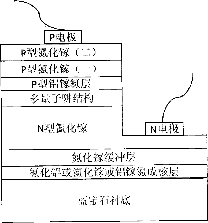
[0019] (1) According to the conventional MOCVD (metal organic chemical vapor deposition) method, grow the LED epitaxial layer structure on the sapphire, PSS or SiC substrate, firstly grow the GaN, AlN or AlGaN nucleation layer on the sapphire, PSS or SiC substrate. Then, a GaN buffer layer, an N-type GaN layer, a light-emitting layer multiple quantum well structure, a P-type AlGaN layer, and a P-type GaN layer are sequentially grown on the nucleation layer. The structure of the prepared epitaxial wafer is as figure 1 Shown. The growth of the P-type GaN layer is divided into two parts. The first part is grown under the conditions of a growth pressure of 100-200torr, a P-type GaN growth rate of 0.5μm / hour--2μm / hour, and a growth temperature of 900℃-1050℃ P-type GaN, the thickness of the P-type GaN in this part is 100nm-300nm, and the secon...


PUM

PropertyMeasurementUnit
refractive indexaaaaaaaaaa

Abstract

The invention provides a method for coarsening the surface of a gallium nitride (GaN)-based light-emitting diode (LED) epitaxial wafer, which comprises the following steps of: (1) preparing an epitaxial wafer, growing a nucleating layer on a substrate epitaxially, growing a GaN buffer layer, an N-type GaN layer, a luminescent layer multi-quantum well structure, a P-type AlGaN layer and a P-type GaN layer on the nucleating layer sequentially, wherein the growth of the P-type GaN layer is divided into two parts; (2) preparing solution of hydrofluoric acid (HF); (3) welding a Pt lead serving as a positive electrode on the surface of the P-type GaN layer by using metal, and connecting a Pt electrode serving as a negative electrode with the HF solution prepared in the step (2); (4) connecting a power supply of 10 to 50 V between the positive electrode and the negative electrode; and (5) corroding, so that an obvious coarsening graph is formed on the surface of the P-type GaN layer. In the method, the coarsened surface of the GaN-based LED epitaxial wafer is prepared by changing the epitaxial growth condition and combining photo-electrochemical (PEC) etching, a process is simple, and the cost is reduced, the coarsening effect is obvious, the light extraction efficiency is high, and the damage of dry etching or high-temperature corrosion to quantum wells is prevented simultaneously.

Description

Technical field [0001] The invention relates to a method for roughening the surface of a gallium nitride-based blue-green light-emitting diode epitaxial wafer, which belongs to the technical field of optoelectronics. Background technique [0002] In recent years, semiconductor light-emitting diodes have received widespread attention, and they have the advantages of small size, high efficiency, and long life. The rapid development of wide band gap III-V semiconductor materials has enabled the commercialization of high-brightness LEDs from green to near-ultraviolet products. At present, light-emitting diodes in the range of ordinary green to ultraviolet are widely used in traffic signal lights, full-color displays, LCD screen backlights, automobile instruments and interior lights. In recent years, ultraviolet light-emitting diodes have entered the market and are mainly used for the detection of biological particles (such as the detection of bacterial spores with an absorption rang...

Claims


Application Information

Patent Timeline
Patent Type & Authority Applications(China)
IPC IPC(8): H01L33/00H01L33/22C30B25/16C30B29/40C30B33/10
Inventor 曲爽邵慧慧王成新李树强徐现刚
Owner HUAWEI TEHCHNOLOGIES CO LTD
Why Eureka
Try Eureka