

Method for manufacturing laser chip for natural gas detection
A manufacturing method, natural gas technology, applied in the direction of lasers, laser components, semiconductor lasers, etc., can solve the problems of high technological content, high price, and inapplicability of natural gas detection in lasers, so as to improve single-mode yield, improve efficiency, The effect of reducing line width
- Summary
- Abstract
- Description
- Claims
- Application Information
AI Technical Summary
Problems solved by technology
Method used
Image

Examples
Embodiment Construction
[0044] In order to make the purpose, content, and advantages of the present invention clearer, the specific implementation manners of the present invention will be further described in detail below in conjunction with the accompanying drawings and embodiments.
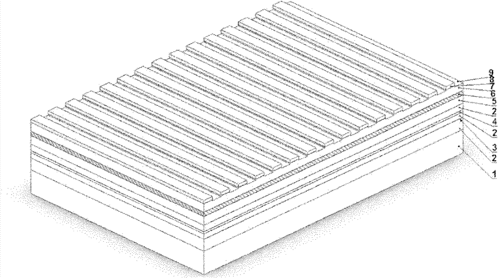
[0045] The manufacturing method of the laser chip for natural gas detection provided by the present invention, such as figure 1 shown, including:
[0046] Step S1:
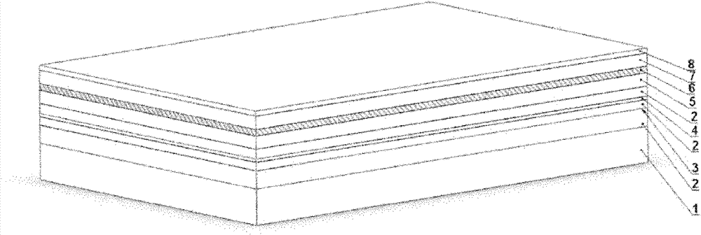
[0047] Such as figure 2 As shown, an epitaxy was performed on an n-InP (n-type indium phosphide) substrate 1 by low-pressure metal-organic chemical vapor deposition. The method has low cost and is suitable for large-scale production; the grown thickness is 1 μm, and the doping concentration is 2×10 18 InP buffer layer 2, InGaAsP (Indium Gallium Arsenide Phosphorus) lower waveguide layer 5 with a thickness of 100nm, InGaAs (Indium Gallium Arsenide) / InGaAsP multi-quantum well structure 6, InGaAsP upper waveguide layer 7 with a thickness of 100nm and a ...
PUM
 Abstract
Description
Claims
Application Information