Method for manufacturing 980nm single-mode wavelength stabilized semiconductor laser

A semiconductor and laser technology, applied in the field of discrete mode semiconductor laser preparation, can solve the problems of highly sensitive collimated beam, complex lithography precision manufacturing process, poor stability, etc.

Inactive Publication Date: 2011-08-10
INST OF SEMICONDUCTORS - CHINESE ACAD OF SCI
View PDF2 Cites 17 Cited by
  • Summary
  • Abstract
  • Description
  • Claims
  • Application Information

AI Technical Summary

Problems solved by technology

[0003] Usually, the methods to achieve stable single-mode wavelength include: DFB and DBR, VCSEL, and external cavity feedback methods, but because the DFB structure requires high lithography precision, the manufacturing process is complicated, and more than two epitaxy is req...

Method used


Image

  • Method for manufacturing 980nm single-mode wavelength stabilized semiconductor laser
  • Method for manufacturing 980nm single-mode wavelength stabilized semiconductor laser
  • Method for manufacturing 980nm single-mode wavelength stabilized semiconductor laser

Examples


preparation example Construction

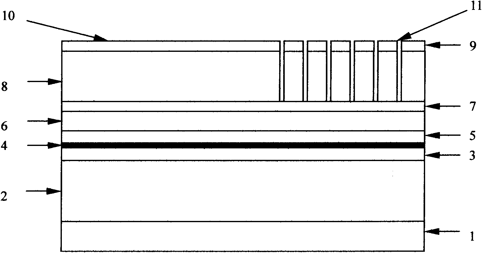
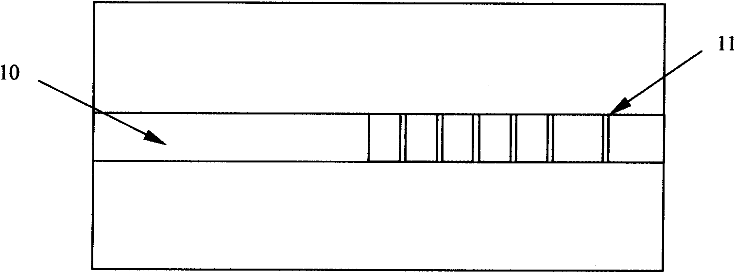
[0024] see figure 1 , figure 2 and image 3 , the invention provides a method for preparing a wavelength-stabilized 980nm single-mode laser, comprising the steps of:

[0025] Step 1: Take a GaAs substrate 1;

[0026] Step 2: Prepare N-type AlGaAs lower confinement layer 2, lower waveguide layer 3, quantum well layer 4, upper waveguide layer 5, first P-type upper confinement layer 6, etch cut-off layer on GaAs substrate 1 in sequence 7. The second P-type upper confinement layer 8 and P-type cap layer 9; wherein the lower confinement layer 2 is a highly doped N-type aluminum gallium arsenic material (Al 0.4 Ga 0.6 As), the Si doping concentration is 1×10 18 cm -3 , with a thickness of 1.5 μm, the purpose is to limit the diffusion of carriers in the active region, so as to reduce the threshold current and improve efficiency; the lower waveguide layer 3 is made of non-doped aluminum gallium arsenic material (A 0.2 Ga 0.8 As) with a thickness of 90nm, the purpose is to enh...

Embodiment

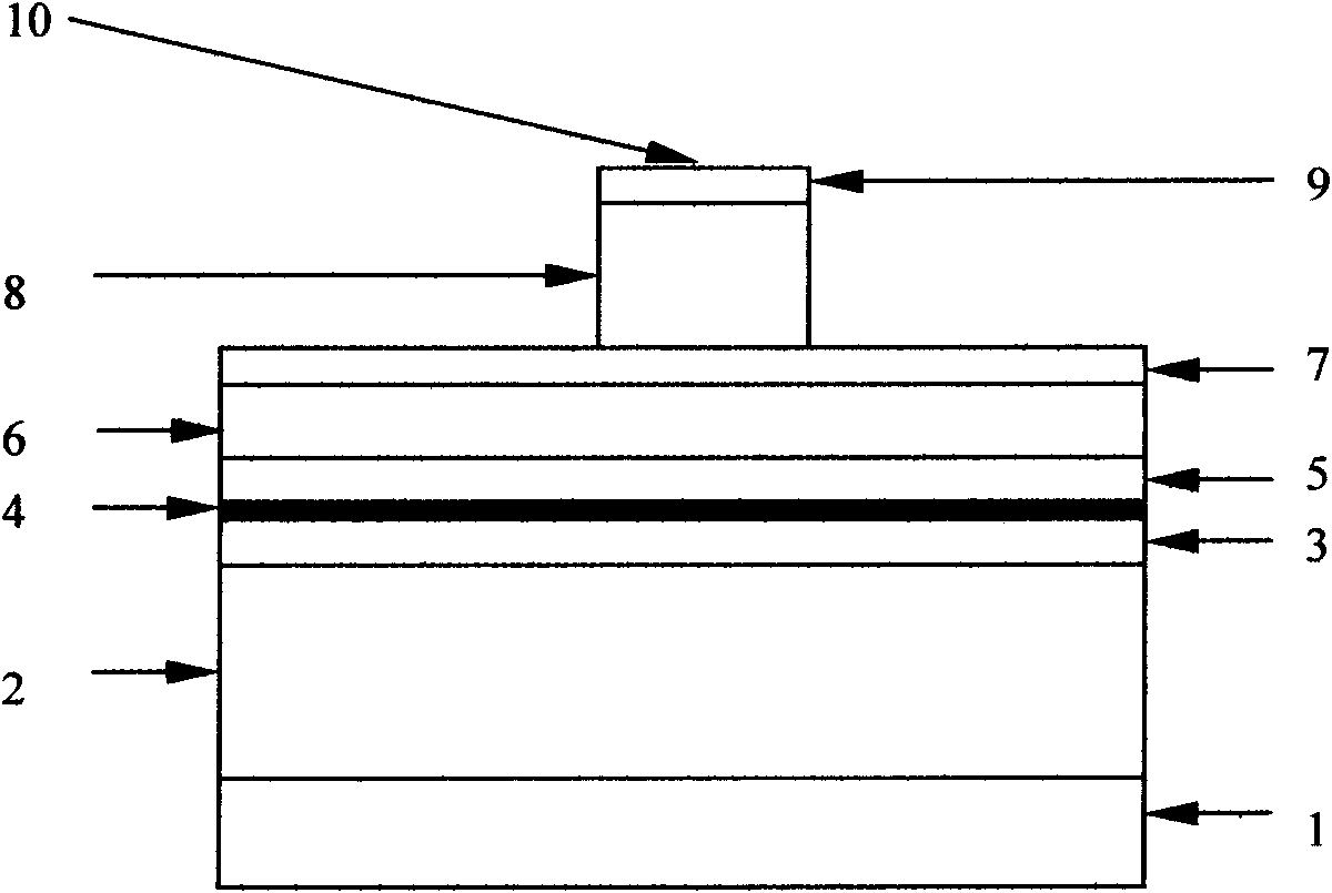
[0030] see again figure 1 , figure 2 and image 3 As shown, the present invention provides a method for preparing a wavelength-stabilized 980nm single-mode laser, comprising the steps of:

[0031] Step 1: Take a GaAs substrate 1;

[0032] Step 2: Prepare N-type AlGaAs lower confinement layer 2, lower waveguide layer 3, quantum well layer 4, upper waveguide layer 5, first P-type upper confinement layer 6, etch cut-off layer on GaAs substrate 1 in sequence 7. The second P-type upper confinement layer 8 and P-type cap layer 9; wherein the lower waveguide layer 3 is made of undoped AlGaAs material, wherein the quantum well layer 4 is made of undoped AlGaInAs material, wherein the upper The waveguide layer 5 is a non-doped AlGaAs material, wherein the first P-type upper confinement layer 6 is a highly doped AlGaAs material with a thickness of 0.3 μm, and the etching cut-off layer 7 is a highly doped P-type InGaP material with a thickness of 20nm, wherein the second P-type uppe...


PUM

PropertyMeasurementUnit
Thicknessaaaaaaaaaa
Thicknessaaaaaaaaaa
Thicknessaaaaaaaaaa

Abstract

The invention provides a method for manufacturing a 980nm single-mode wavelength stabilized semiconductor laser, which comprises the following steps of: 1, providing a gallium arsenide substrate; 2, sequentially preparing a lower N-type aluminum gallium arsenide limiting layer, a lower waveguide layer, a quantum well layer, an upper waveguide layer, a first upper P-type limiting layer, an etchingstopping layer, a second upper P-type limiting layer and a P-type cap layer on the gallium arsenide substrate; 3, preparing an etched mask pattern on the surface of the P-type cap layer by adopting aphotoetching technology; and 4, performing downward etching on the P-type cap layer to form a ridge waveguide structure, and simultaneously performing longitudinal etching until reaching the surface of the etching stopping layer on one side of the upper surface of the ridge waveguide structure to form a plurality of aperiodically distributed groove structures to finish the manufacturing of the laser.

Description

technical field [0001] The invention relates to the field of semiconductor lasers, in particular to a preparation method for a discrete-mode semiconductor laser (DMLD) that realizes 980nm dynamic single-mode wavelength stability. Background technique [0002] 980nm semiconductor lasers are widely demanded and applied as the pump source of solid-state lasers and in the fields of fiber lasers, sensing, and medical treatment. However, with the continuous increase of temperature and operating current, the center wavelength of semiconductor lasers drifts. This is a big hurdle for pumping applications with small absorption bandwidths. Therefore, it is particularly urgent and crucial to ensure stable and effective pumping of solid-state lasers with narrow absorption bandwidths in the entire working range, and to improve the spectral characteristics of semiconductor lasers such as spectral purity and wavelength stability. [0003] Usually, the methods to achieve stable single-mode ...

Claims


Application Information

Patent Timeline
IPC IPC(8): H01S5/22H01S5/24H01S5/343
Inventor 高卓王俊李全宁马骁宇
Owner INST OF SEMICONDUCTORS - CHINESE ACAD OF SCI
Why Eureka
Try Eureka