MEMS (Micro Electro Mechanical System) microphone and pressure integration sensor, and manufacturing method thereof

A technology integrating sensors and microphones, which is applied in the direction of sensors, electrostatic transducer microphones, semiconductor electrostatic transducers, etc., can solve the problems of complex packaging process, large device size, and high cost, so as to improve standardization and unification, and improve signal quality. Excellent noise ratio performance and high anti-interference ability

Active Publication Date: 2011-08-17
MEMSEN ELECTRONICS
View PDF3 Cites 63 Cited by
  • Summary
  • Abstract
  • Description
  • Claims
  • Application Information

AI Technical Summary

Problems solved by technology

[0006] However, the problem is that in the above-mentioned traditional manufacturing methods of capacitive pressure sensors and microphone sensors, whether it is a pressure sensor chip or a microphone sensor chip, they are separated from the conductor connection chip or the signal processing circuit chip, and each chip is manufactured separately. Packaging process integration, whether it is a plastic package with

Method used


Image

  • MEMS (Micro Electro Mechanical System) microphone and pressure integration sensor, and manufacturing method thereof
  • MEMS (Micro Electro Mechanical System) microphone and pressure integration sensor, and manufacturing method thereof
  • MEMS (Micro Electro Mechanical System) microphone and pressure integration sensor, and manufacturing method thereof

Examples


Example Embodiment

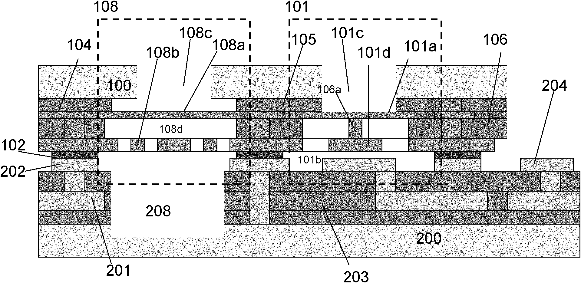
[0089] In the first embodiment, a part of the backside of the first substrate 100 is exposed outside the package. In other words, the first opening 108c and the second opening 101c serve as the inlets for sound and pressure, respectively, and introduce sound waves and pressure changes into the sensitive film and the sensing film. Above, different sound and pressure inlet designs can also be used, as detailed in the following examples.

Example Embodiment

[0090] Embodiment 2

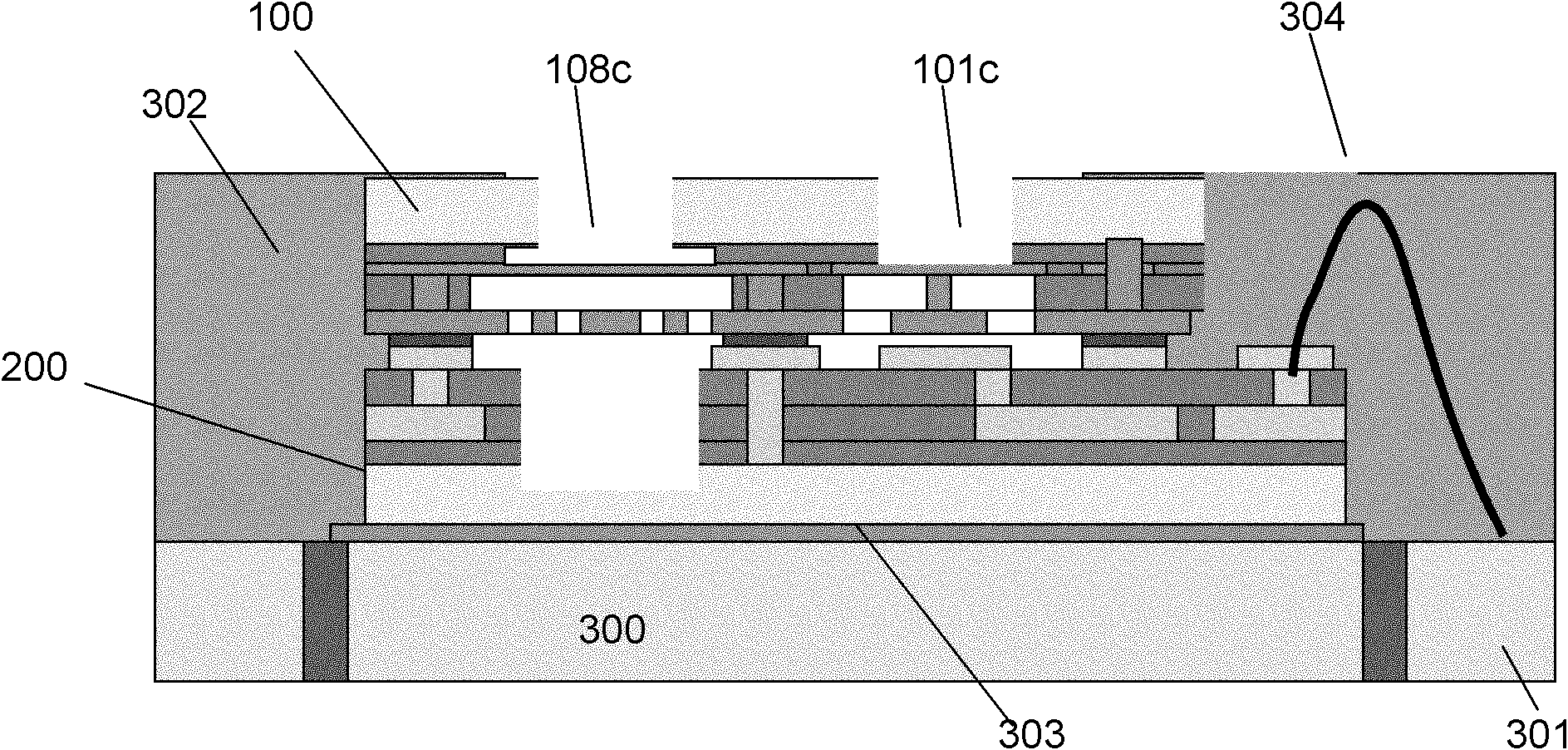
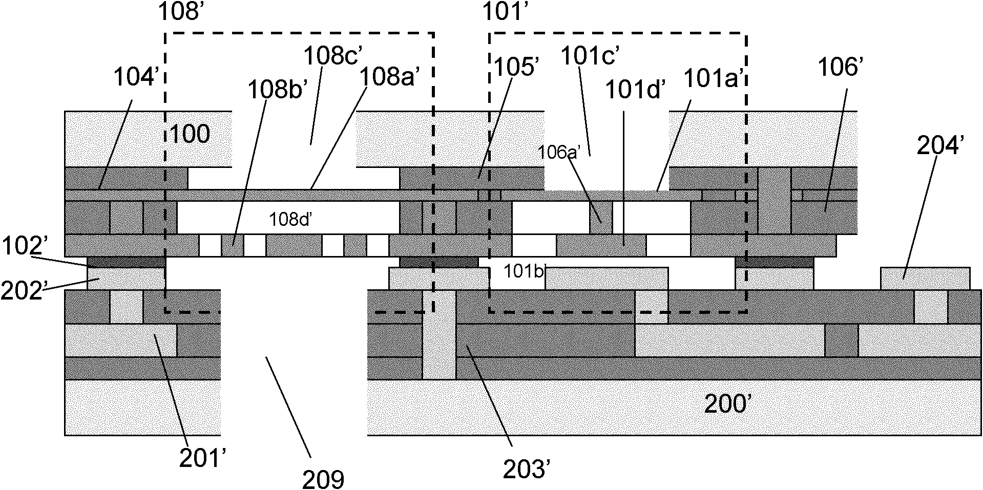
[0091] image 3 It is a schematic structural diagram of the MEMS microphone and the pressure integrated sensor described in this embodiment, Figure 4 for image 3 Schematic diagram of the package structure of the integrated sensor.

[0092] As shown in the figure, the difference between the MEMS microphone and the pressure integrated sensor is that the second substrate 200' has a third opening 109 on the back side (facing away from the first substrate 100'), which is different from the above-mentioned embodiment. The position of the sensitive film 108c' of the microphone unit corresponds to the position of the cavity 108d', and the sensitive film 108a' and the back plate electrode 108b' both have through holes, so the first opening 108c', the cavity 108d' and The third opening 209 forms a through channel in the first substrate 100' and the second substrate 200', which can simultaneously serve as a sound and pressure transmission channel.

[0093] Aft...

Example Embodiment

[0103] Embodiment 3

[0104] The manufacturing method of the MEMS microphone and the pressure sensor in the first embodiment will be described in detail below with reference to the accompanying drawings. Figure 5 It is a flowchart of the manufacturing method of the MEMS microphone and the pressure sensor described in the embodiment of the present invention, Figure 6 to Figure 13 It is a schematic diagram of the manufacturing method of the MEMS pressure sensor. As shown in the figure, the manufacturing method includes:

[0105] Step S1 : providing a first substrate, and forming the sensing film of the capacitive pressure sensing unit, the sensitive film of the microphone unit and the first adhesive layer on the surface of the first substrate on the first substrate.

[0106] Specifically, as Image 6 As shown, first, the first substrate 100 includes a silicon substrate, and a first dielectric layer 105 is formed on the silicon substrate. Preferably, the first dielectric lay...


PUM


Abstract

The invention relates to an MEMS (Micro Electro Mechanical System) microphone and pressure integration sensor and a manufacturing method thereof. The sensor provided by the invention comprises a first substrate and a second substrate, wherein the first substrate is provided with an induction film of a capacitance pressure sensing unit, a sensitive film of a microphone unit and a first bonding layer on the surface of the first substrate; the second substrate is provided with a dielectric layer between conductors, a conductor wiring layer positioned in the dielectric layer between the conductors and/or a second bonding layer on the surface of the second substrate; the second substrate and the first substrate are oppositely arranged and fixedly connected through the first bonding layer and the second bonding layer; and the patterns of the first bonding layer and the second bonding layer correspond to each other and are conductive materials. In the MEMS microphone and pressure sensor and the manufacturing method thereof provided by the invention, the capacitance pressure sensing unit and the microphone unit through the two substrates, thus the sensor and method provided by the invention are suitable for chip structures produced in a large scale and integrated with various MEMS sensors, are beneficial to the compatibility with an integrated circuit process, have the advantages that the standardization of a manufacturing process and a packaging process is enhanced, the volumes of devices are small, the signal-to-noise ratio performance is excellent, and the interference resistance is high.

Description

technical field [0001] The invention relates to a microelectronic mechanical system technology, in particular to a MEMS microphone and a pressure integrated sensor and a manufacturing method thereof. Background technique [0002] In recent years, various MEMS sensors have been used more and more in mobile phones and other portable electronic products, such as MEMS microphones, pressure sensors and gyroscopes, replacing traditional sensors with their miniaturization and thinness. In particular, the rapid development of smartphones has driven the market demand for various MEMS sensors, and the growing ecosystem of smartphone application software is largely due to MEMS sensors. [0003] MEMS microphones are miniature microphones made by etching pressure-sensing diaphragms on semiconductors through a microelectromechanical system process, and are commonly used in mobile phones, headphones, notebook computers, cameras, and automobiles. Driven by the requirement of compatibility ...

Claims


Application Information

Patent Timeline
IPC IPC(8): H04R19/04H04R31/00
CPCH04R19/04H04R31/006H04R19/005
Inventor 柳连俊
Owner MEMSEN ELECTRONICS
Why Eureka
Try Eureka