Method for patterning sapphire by combining wet etching and dry etching

A patterned sapphire and wet etching technology, which is applied in the manufacture of discharge tubes, electrical components, semiconductors/solid-state devices, etc., can solve the problems of difficult control of etching rate, difficulty in epitaxial growth, high cost, etc., and overcome the wet etching rate The effect of instability, stable dry etch rate, and low volume production cost

Active Publication Date: 2012-11-07
HC SEMITEK CORP
View PDF0 Cites 2 Cited by
  • Summary
  • Abstract
  • Description
  • Claims
  • Application Information

AI Technical Summary

Problems solved by technology

However, when patterned substrates are prepared by dry etching, there are disadvantages such as low etching rate, high cost, and high damage to materials.
Relatively speaking, wet etching is easy to operate, low in etching cost, and fast in etching rate, and can be used in mass production, but its etching accuracy is not high, the etching rate is difficult to control, and it is easy to form side etching. It is difficult to prepare high-quality, high precision graphics
More importantly, wet etching will form multiple crystal planes, and nitrides need to grow on specific crystal planes, so wet etching will cause difficulties in epitaxial growth

Method used


Image

  • Method for patterning sapphire by combining wet etching and dry etching
  • Method for patterning sapphire by combining wet etching and dry etching
  • Method for patterning sapphire by combining wet etching and dry etching

Examples


Embodiment 1

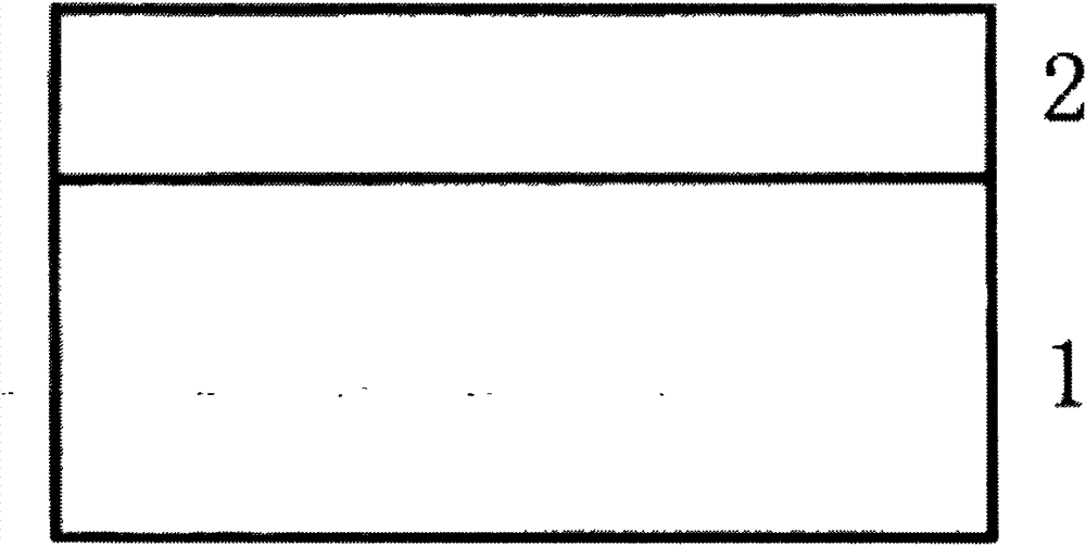
[0020] First, a 0.5um silicon dioxide film 2 is deposited on a 2-inch C-plane sapphire substrate 1 by plasma-enhanced chemical vapor deposition (PECVD), and the structure profile after deposition is as follows figure 1 shown;

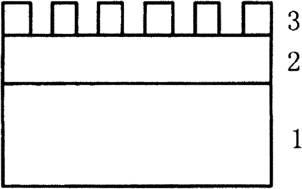
[0021] Next, a photoresist layer 3 is coated on the silicon dioxide film 2 using conventional photolithography techniques, and a circular array is formed by exposure and development. The size and spacing of the circular array unit structure is 2um, and the structural section after photolithography is as follows figure 2 shown;

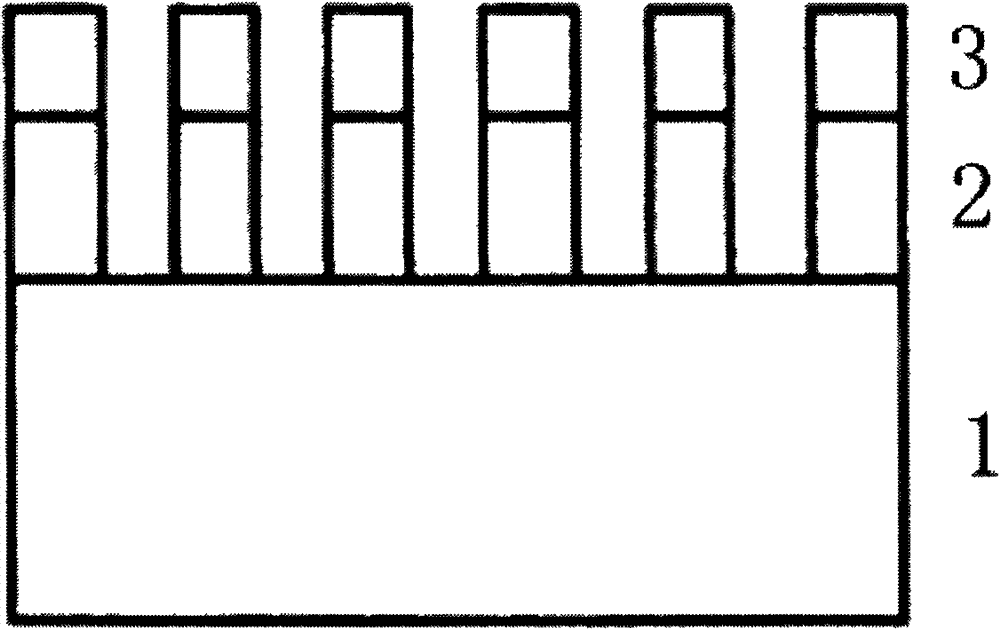
[0022] Then, using hydrofluoric acid + ammonium fluoride + H 2 O mixed solution, the photolithography pattern is etched on the silicon dioxide film 2, and its structural section is as follows image 3 shown;

[0023] Subsequently, using the silicon dioxide film 2 as a pattern mask, first use a mixture of sulfuric acid and phosphoric acid with a volume ratio of 3:1 to etch the C-plane sapphire substrate 1 at 260°C to a depth...


PUM

PropertyMeasurementUnit
thicknessaaaaaaaaaa
thicknessaaaaaaaaaa

Abstract

The invention discloses a method for patterning a sapphire substrate by combining wet etching and dry etching. The method comprises the following steps of: depositing a layer of silicon dioxide film on the sapphire substrate; preparing a photoresist masking film with a pattern on the silicon dioxide film through lithography; etching the lithography pattern onto the silicon dioxide film; etching the pattern onto the sapphire substrate by a method of combining wet etching and short-time dry etching, wherein the patterned silicon dioxide film serves as a masking film; and removing the silicon dioxide film through wet etching, cleaning the sapphire substrate and finishing the preparation of the patterned sapphire substrate. Because of the combination of wet etching and dry etching and the optimization of related technical parameters, the etching speed is guaranteed, the etching cost is reduced, better pattern precision can be achieved, and good etching effect can be achieved. The patterned sapphire substrate can be applied to the epitaxial growth of nitrides with low dislocation density and high crystal quality.

Description

technical field [0001] The invention relates to the technical field of semiconductors, in particular to a method for patterning a sapphire substrate by combining wet etching and dry etching. Background technique [0002] In the past ten years, nitride compound semiconductor materials represented by III-V gallium nitride (GaN) have gained a lot of attention because of their wide direct bandgap, high thermal conductivity, high hardness, low dielectric constant, and radiation resistance. People's widespread attention has great application potential in solid-state lighting, solid-state lasers, optical information storage, ultraviolet detectors and other fields. At present, major breakthroughs have been made in the field of GaN devices in the world. High-brightness blue and green light-emitting diodes (LEDs) have already been commercialized, and long-life ultraviolet and blue lasers have also been successfully developed. Due to the lack of suitable substrate materials, epitaxial...

Claims


Application Information

Patent Timeline
Patent Type & Authority Patents(China)
IPC IPC(8): H01L21/02H01J37/32
Inventor 张建宝顾小云
Owner HC SEMITEK CORP
Why Eureka
Try Eureka