Method for preparing nanometer imaging substrate of LED (light emitting diode) chip epitaxial growth

An LED chip and nano-pattern technology, applied in electrical components, circuits, semiconductor devices, etc., can solve problems such as the inability to meet the light extraction efficiency of LED devices, and achieve the effect of good periodicity and uniform pattern

Active Publication Date: 2011-10-12
黄山博蓝特半导体科技有限公司
View PDF1 Cites 3 Cited by
  • Summary
  • Abstract
  • Description
  • Claims
  • Application Information

AI Technical Summary

Problems solved by technology

The traditional patterned sapphire substrate (CPSS-Conventional Patterned Sapphire Substrate) technology is limited by the photolithography process, and the

Method used


Image

  • Method for preparing nanometer imaging substrate of LED (light emitting diode) chip epitaxial growth
  • Method for preparing nanometer imaging substrate of LED (light emitting diode) chip epitaxial growth
  • Method for preparing nanometer imaging substrate of LED (light emitting diode) chip epitaxial growth

Examples


Embodiment Construction

[0022] In order to further illustrate content of the present invention, below in conjunction with embodiment and accompanying drawing, the present invention is described in detail:

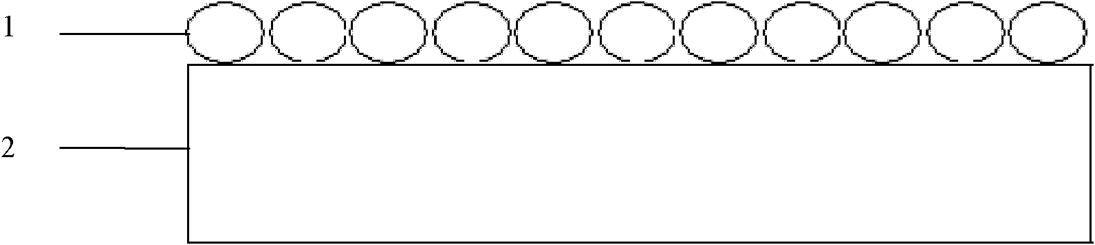
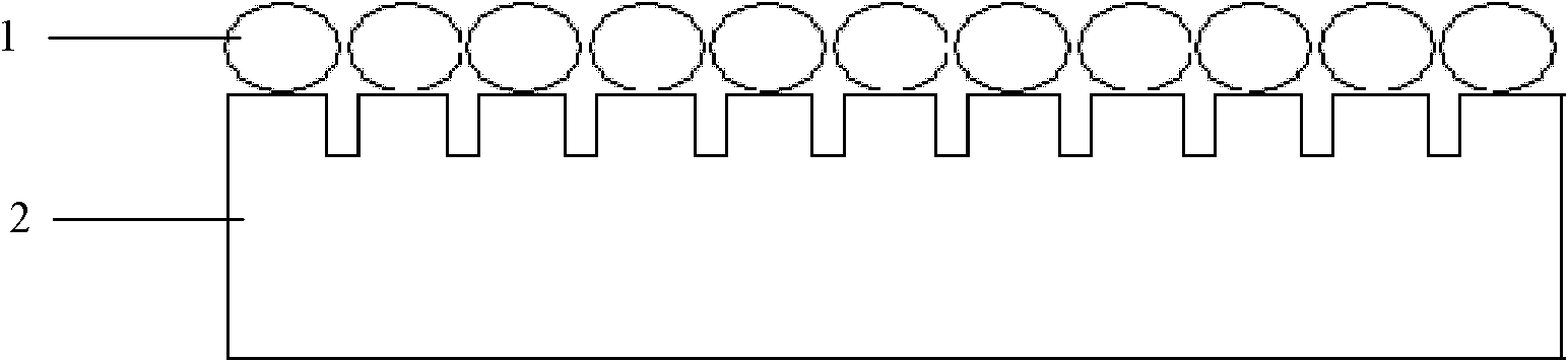
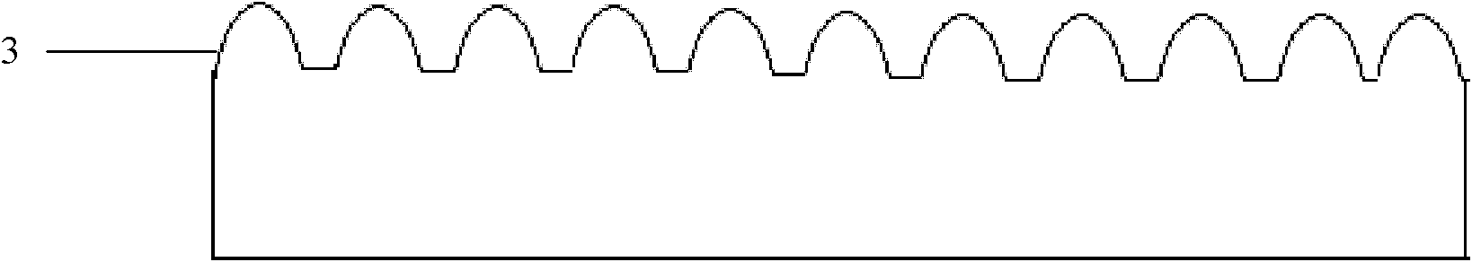
[0023] A method for preparing a nano-patterned substrate for LED chip epitaxial growth, the specific method is as follows:

[0024] 1. The sapphire substrate is firstly cleaned in a mixed solution of sulfuric acid:hydrogen peroxide=4:1, and rotated for 4 minutes. Then in HF:H 2 Sonicate for 2 min in a mixed solution of O=1:1. Finally, rinse with deionized water, N 2 Clean the surface and dry it in a drying oven (80°C).

[0025] 2. After adding 2ml of deionized water and 6ml of ammonia water to 50ml of absolute ethanol solution, slowly drop in 4ml of tetraethyl orthosilicate (TEOS) at a rate of about 200 microliters every two minutes, and react for 18-24 hours. During this period, the magnetic stirrer kept stirring at a constant speed, and the rotating speed was 300 rpm. After the reaction is ...


PUM


Abstract

The invention belongs to the field of solid illumination, and in particular relates to a method for preparing a nanometer patterned substrate of LED (light emitting diode) chip epitaxial growth. The method particularly comprises the following steps: dropping silicon oxide nanometer balls which are dispersed uniformly on a sapphire substrate after cleaning treatment, and coating the silicon oxide nanometer balls on the surface of the sapphire substrate uniformly by utilizing a spin coating machine in a single layer mode; carrying out ICP (inductively coupled plasma) etching processing on the sapphire substrate which takes the silicon oxide nanometer balls as masks, and dividing the etching into two groups: firstly, etching the image depth of the nanometer patterned substrate by utilizing BC13 gas; and then etching the image width of the nanometer patterned substrate by utilizing BC13, C12, and Ar gas; and taking the sapphire substrate out after etching, and drying for use after corrosion and cleaning. According to the invention, the dislocation density in the LED chip can be reduced effectively, the occurrence of cracking can be avoided, the crystalline quality and uniformity of epitaxial materials can be improved, the probability of light emission of the light for the LED from the sapphire substrate is increased, and further the light-emitting efficiency of the LED chip can beimproved.

Description

technical field [0001] The invention belongs to the field of solid-state lighting, in particular to a method for preparing a nano-patterned substrate for LED chip epitaxial growth. Background technique [0002] Lighting has always been closely related to the civilization and progress of human society, from the use of fire in primitive society, to Edison's invention of incandescent lamps in 1886, and then fluorescent lamps are widely used in industrial and civil lighting. The production and social activities of human beings have been extended to the whole day, which has greatly promoted the progress of human civilization. However, the current lighting sources represented by fluorescent lamps have a series of defects, such as low luminous efficiency, high energy consumption, short service life, and the generation of toxic waste of heavy metals such as mercury, which are far from meeting the requirements of modern society for high efficiency, energy saving, and environmental pr...

Claims


Application Information

Patent Timeline
IPC IPC(8): H01L33/00
Inventor 刘建哲李京波李庆跃李凯颜晓升池旭明李树深夏建白
Owner 黄山博蓝特半导体科技有限公司
Why Eureka
Try Eureka