

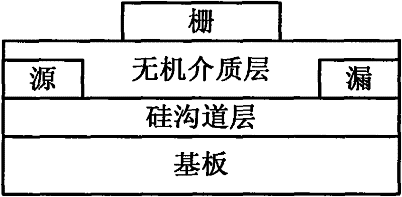
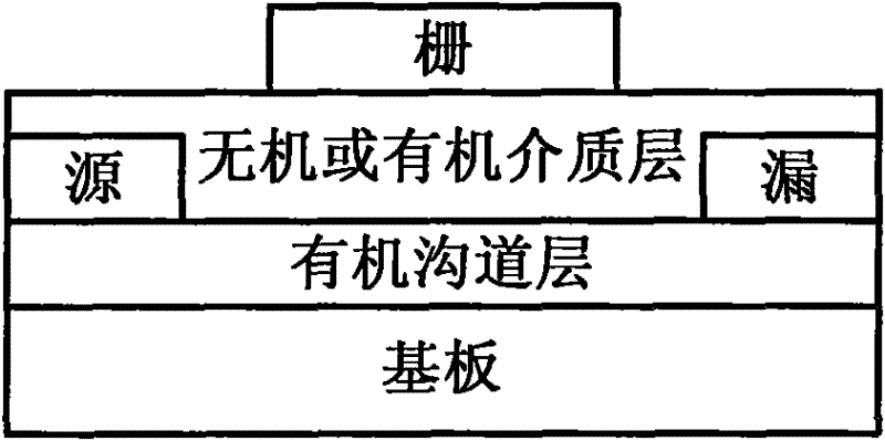
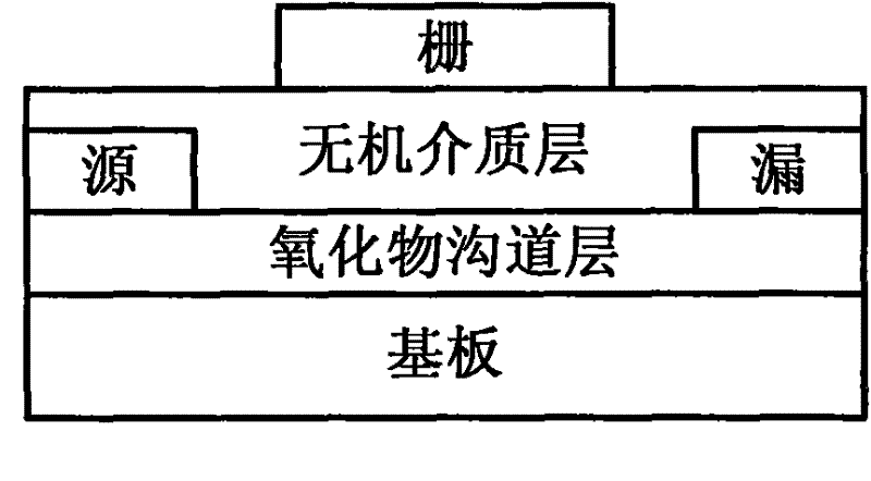
Mixed structure thin-film transistor taking oxide semiconductor as channel layer
An oxide semiconductor, thin film transistor technology, applied in transistors, semiconductor devices, electrical components, etc., can solve the problems of unsuitable flexible display screens, high dielectric layer process temperature, good electrical performance, easy low temperature and large area preparation, The effect of good application prospects
- Summary
- Abstract
- Description
- Claims
- Application Information
AI Technical Summary
Problems solved by technology
Method used
Image

Examples
specific Embodiment
[0022] The indium-zinc alloy target (In:Zn=0.586:1 atomic ratio) is selected, and the reaction chamber is vacuumed to below 2×10⁻³Pa before a-IZO film deposition, and then the O 2 and Ar gas are passed into the reaction chamber in sequence, and the oxygen partial pressure in the reaction chamber is controlled to be 5.0×10 -2 Pa, the working pressure is 3.0×10 -1 Pa. The sputtering current and the sputtering voltage were adjusted to 120mA and 300V respectively, and the sputtering time was 10 minutes to form a thin film on a common glass sheet. The thickness of the film is about 110nm, and the resistivity is greater than 1×10 4 Ω·cm, the average transmittance of visible light is greater than 82%.
[0023] 80nm aluminum films were prepared as source-drain electrodes by reactive magnetron sputtering with aluminum oxide masks with aspect ratios of 500μm / 100μm and 400μm / 40μm. The sputtering current was 100mA and the sputtering voltage was 350V.
[0024] A 20 mg / ml polytetravinyl...
PUM
 Abstract
Description
Claims
Application Information