Copper palladium alloy monocrystal bonding wire and manufacturing method thereof

A palladium alloy and bonding wire technology, which is applied in the field of copper-palladium alloy single crystal bonding wire and its manufacturing, can solve the problems of low hardness of electroplating layer, poor resistance to friction, poor high temperature stability and high production cost, and can shorten the welding distance, Good anti-oxidation performance and improved bonding strength

Active Publication Date: 2011-10-26
江西蓝微电子科技有限公司
View PDF6 Cites 14 Cited by
  • Summary
  • Abstract
  • Description
  • Claims
  • Application Information

AI Technical Summary

Problems solved by technology

[0003] The purpose of the present invention is to provide a copper-palladium alloy single crystal bonding wire and its manufacturing method, which overcomes the problems of easy oxidation of the surface of the existing alloy-type bonding copper wire, poor high-temperature stability, and wire breakage during drawing, and the problems of gold-plated bonding wire. The defects and deficiencies of high production cost of copper wire, low hardness of elec

Method used


Image

  • Copper palladium alloy monocrystal bonding wire and manufacturing method thereof
  • Copper palladium alloy monocrystal bonding wire and manufacturing method thereof

Examples


Example Embodiment

[0019] Embodiment one

[0020] ① Extraction of high-purity copper: Dilute the copper nitrate solution with high-purity water at a ratio of 1:4 to prepare an electrolyte; use the national standard No. 1 pure copper as the anode to immerse in the electrolyte, and ensure that 95% of the volume ratio of pure copper is immersed in the electrolysis liquid; use high-purity copper foil as the cathode to immerse in the electrolyte, and also ensure that high-purity copper foil with a volume ratio of 955 is immersed in the electrolyte; input 7-9V, 2.5-3.5A direct current between the anode and cathode to Supplement fresh electrolyte to keep the temperature of the electrolyte not exceeding 60°C; when the cathode accumulates high-purity copper with a purity greater than 99.9995%, replace the high-purity copper foil in time, and then clean and dry it for later use.

[0021] ② Copper-palladium alloy rod: In a continuous casting room for horizontal continuous casting of metal single crystal wi...

Example Embodiment

[0029] Embodiment two

[0030] Step 1. to step 4. are the same as in Embodiment 1.

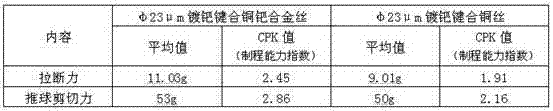
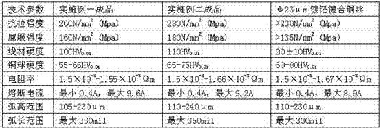
[0031] ⑤Palladium plating on the surface: Apply conventional electroplating equipment and technology to electroplate pure palladium anti-oxidation protective layer on the φ0.2mm copper-palladium alloy wire after annealing. The purity of palladium for electroplating is required to be greater than 99.999%; the current density is 4-4.5A / dm 2 , the speed of copper wire is 4-5m / min, and the thickness of the coating is controlled at 2μm-7μm; for copper-palladium alloy wire products after palladium plating, the sum of the weight of palladium inside the single crystal copper-palladium alloy and pure palladium on the surface accounts for the percentage of the total weight Controlled at 1.35%-10.18%; the rest is copper, and the rest is copper.

[0032] ⑥Precise drawing: Using conventional drawing equipment and technology, the φ0.2mm copper-palladium alloy wire plated with pure palladium anti-oxidation pr...


PUM

PropertyMeasurementUnit
Thicknessaaaaaaaaaa

Abstract

A copper palladium alloy monocrystal bonding wire and a manufacturing method thereof are disclosed. Base material of the copper palladium monocrystal bonding wire comprises, by weight, 1.35%-10.18% of palladium, 0.0001%-0.0003% of Calcium, 0.0002%-0.0008% of Rhenium and the balance copper. The manufacturing method comprises the following steps: extracting high purity copper and high purity palladium; preparing monocrystalline copper palladium alloy rod; plating palladium on surface; coarse drawing and fine drawing; carrying out a heat treatment; cleaning the surface; shunting winding. The invention abandons the traditional technique: drawing firstly and then electroplating. In the method of the invention, the monocrystalline copper palladium alloy wire with a wire diameter of less than 3mm is produced, then palladium layer is electroplated, and finally, the palladium copper alloy bonding wire finished product is produced by drawing. By using the invention, oxidation resistance of bonding copper wire can be effectively raised; the oxidation resistance of the bonding copper wire can be equal to the oxidation resistance of bonding gold wire; shelf-life of the bonding copper wire product after being sealed off can be substantially prolonged. Mechanical strength of alloy finished products which are added elements, such as palladium, calcium, rare earth and the like, can be higher than materials produced by other ways, which is beneficial to further reduce the wire diameter of the bonding wire and shorten welding spacing, and is suitable for integrated circuit package with high-density and multi-pin.

Description

technical field [0001] The invention relates to a metal bonding wire and a manufacturing method thereof for a microelectronic subsequent packaging process, in particular to a copper-palladium alloy single crystal bonding wire and a manufacturing method thereof. Background technique [0002] The bonding process of microelectronic device chips refers to welding the two ends of the bonding wire to the chip pads and lead frame pins respectively by ultrasonic pressure at a certain temperature to realize the connection between the internal circuit of the chip and the external circuit. Early bonding wires were mostly made of pure gold, but with the increasing scarcity of gold resources and rising prices, the cost of microelectronic packaging has risen sharply. Therefore, people in the industry have successfully developed copper wire products to replace expensive gold wire products. . These bonding copper wires are cheap and superior to gold wires in terms of tensile, shear strengt...

Claims


Application Information

Patent Timeline
IPC IPC(8): H01L23/49H01L21/48C30B29/52C25D3/50C25D7/06C22F1/08B21C1/02
CPCH01L24/43H01L2224/43H01L2224/43848H01L2224/45H01L2224/45015H01L2224/45144H01L2224/45147H01L2224/45565H01L2224/45664H01L2924/00011H01L2924/00014H01L2924/0102H01L2924/01029H01L2924/01033H01L2924/01046H01L2924/01047H01L2924/01075H01L2924/01078H01L2924/01079H01L2924/01105H01L2924/14H01L2924/00015H01L2924/013H01L2924/00H01L2224/48H01L2924/20109H01L2924/2011H01L2924/20111H01L2924/01006H01L2924/00012H01L2924/01004H01L2924/20751H01L2924/20752H01L2924/20753H01L2924/20754H01L2924/20755H01L2924/01205
Inventor 徐云管彭庶瑶
Owner 江西蓝微电子科技有限公司
Why Eureka
Try Eureka