

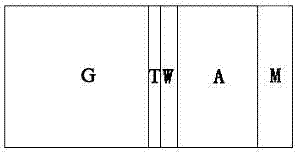
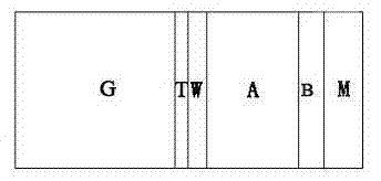
CdTe solar cell by using V-Se film as back contact layer
A technology for solar cells and vanadium selenide, applied in circuits, photovoltaic power generation, electrical components, etc., can solve the problems of complex composition and structure of tellurium-copper phase, battery performance degradation, etc.
- Summary
- Abstract
- Description
- Claims
- Application Information
AI Technical Summary
Problems solved by technology
Method used
Image

Examples
Embodiment 1
[0018] (1) Preparation of V-Se thin film
[0019] Put the sample into the vacuum chamber with a vacuum of 10 -4 pa, the sample temperature is room temperature, and the electron beam evaporation method is used to alternately evaporate vanadium and selenium, wherein the purity of vanadium is 99.999%, and the purity of selenium is 99.97%. The thickness of deposited vanadium is 1~10 nm, the thickness ratio of vanadium and selenium is 0.26, and the total thickness of V-Se film is 80 nm;
[0020] (2) Post-treatment V-Se thin film
[0021] Take out the sample deposited with V-Se thin film, put it into a vacuum annealing furnace protected by nitrogen or inert gas, and carry out post-treatment at a temperature of 250 0 C~300 0 C, the time is 10~60 minutes, and then naturally cooled to room temperature, that is, to obtain VSe 2-x (x=0) Sample of thin film.
Embodiment 2
[0023] (1) Preparation of V-Se thin film
[0024] Put the sample into the vacuum chamber with a vacuum of 10 -4 pa, the sample temperature is 300 0 C, using the electron beam evaporation method to alternately evaporate vanadium and selenium, wherein the purity of vanadium is 99.999%, and the purity of selenium is 99.97%. The thickness of deposited vanadium is 1~10 nm, the thickness ratio of vanadium and selenium is 0.26, and the total thickness of V-Se film is 100 nm;
[0025] (2) Post-treatment V-Se thin film
[0026] In a vacuum chamber, keep the sample warm for 10-60 minutes, and then naturally cool to room temperature, that is, to obtain 2-x (x=0) Sample of thin film.
Embodiment 3
[0028] (1) Install the target and sample
[0029] Fix the vanadium target (purity 99.99% and above) and the selenium target (purity 99.99% and above) on the two target positions corresponding to the sputtering device, fix the sample on the substrate position, and adjust the target and substrate. The distance is 6~9 cm;
[0030] (2) Preparation of V-Se thin film
[0031] In-situ growth of V-Se thin film, that is, first heating the sample temperature to 300 0 C, followed by co-sputtering vanadium and selenium to obtain V-Se thin films, in which the background vacuum ~10 -4 Pa, the working gas is argon, the working pressure is 0.1~3.5 Pa, the sputtering power of vanadium target is 30~300 W, the sputtering power of selenium target is 30~100 W, the sputtering rate V / Se is 0.26~0.27, and the sputtering thickness is 70 nm;
[0032] (3) Post-treatment V-Se thin film
[0033] After the sputtering is completed, keep the pressure in the sputtering chamber for 10-60 minutes under th...
PUM
 Abstract
Description
Claims
Application Information