
Method for depositing silicon membrane for solar cell on basis of magnetic control sputtering technology

A solar cell and magnetron sputtering technology, which is applied in sputtering plating, ion implantation plating, coating, etc., can solve the problem of complex safety control process, difficulty in precise control of hydrogen content, and dense structure of amorphous silicon film. Improve the density and deposition rate, facilitate control, and lower the investment threshold

Inactive Publication Date: 2013-01-02
XIAN UNIV OF TECH
View PDF0 Cites 0 Cited by
  • Summary
  • Abstract
  • Description
  • Claims
  • Application Information

AI Technical Summary

Problems solved by technology

[0004] At present, when preparing silicon thin films for silicon-based thin-film solar cells, the industry uses plasma-enhanced chemical vapor deposition (PECVD) as the preparation method, and special gases such as triane (silane, borane, and phosphine) as the main raw materials. The production process The safety control is extremely strict and the process flow is relatively complicated. At the same time, the structure of the amorphous silicon thin film is not good enough, and the hydrogen content is difficult to accurately control.

Method used


Image

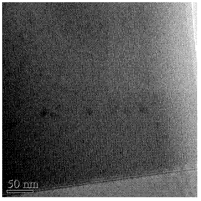
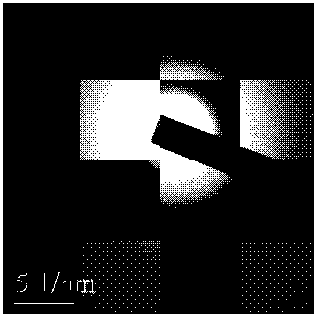
  • Method for depositing silicon membrane for solar cell on basis of magnetic control sputtering technology
  • Method for depositing silicon membrane for solar cell on basis of magnetic control sputtering technology
  • Method for depositing silicon membrane for solar cell on basis of magnetic control sputtering technology

Examples


Embodiment 1

[0024] The equipment used in this embodiment mainly includes magnetron sputtering equipment. The vacuum chamber of the magnetron sputtering equipment includes at least one working vacuum chamber and a plurality of auxiliary vacuum chambers connected to both sides of the working vacuum chamber. A high-purity solid silicon target is set in the chamber, and a tooling frame is installed horizontally through the entire vacuum chamber, and a driving device is connected to the tooling frame. The driving device is used to drive the tooling frame to make a continuous straight line along the direction of the vacuum chamber in the vacuum chamber. sports.

[0025] A method of depositing a silicon thin film for solar cells based on magnetron sputtering technology of the present invention, specifically comprises the following steps:

[0026] Step 1: Select conductive glass as the substrate, and perform pre-cleaning treatment on the substrate.

[0027] The specific method for pretreatment c...

Embodiment 2

[0035] The equipment used in this embodiment is the same as in Embodiment 1.

[0036] A method of depositing a silicon thin film for solar cells based on magnetron sputtering technology of the present invention, specifically comprises the following steps:

[0037] Step 1: Select a durable and flexible polymer material as the base material, specifically select plastic with electrodes pre-plated as the base material, and perform pre-cleaning treatment on the base material.

[0038] The specific method for pretreatment cleaning of the substrate is: put the substrate in a solution containing a cleaning agent, and perform ultrasonic cleaning to remove stains on the surface of the substrate; then put the substrate in deionized water, and perform ultrasonic cleaning to remove residual detergent and dry with hot air.

[0039] Step 2: Place the substrate cleaned before step 1 on the tooling frame, and control the distance between the substrate on the tooling frame and the silicon targ...

Embodiment 3

[0045] The equipment used in this embodiment is the same as in Embodiment 1.

[0046] A method of depositing a silicon thin film for solar cells based on magnetron sputtering technology of the present invention, specifically comprises the following steps:

[0047] Step 1: Select conductive glass as the substrate, and perform pre-cleaning treatment on the substrate.

[0048] The specific method for pretreatment cleaning of the substrate is: place the substrate in a solution containing a cleaning agent, and clean it with a mechanical brush to remove stains on the surface of the substrate; then put the substrate in deionized water and ultrasonically clean it to Remove residual cleaning agent and dry with hot air.

[0049] Step 2: Place the substrate cleaned before step 1 on the tooling rack, and control the distance between the substrate on the tooling rack and the silicon target to be 110 mm. The substrate is sent to the vacuum chamber of the magnetron sputtering equipment throu...


PUM

PropertyMeasurementUnit
thicknessaaaaaaaaaa
thicknessaaaaaaaaaa
thicknessaaaaaaaaaa

Abstract

The invention relates to a method for depositing a silicon membrane for a solar cell on the basis of the magnetic control sputtering technology. The prepared silicon membrane is between 0.01 and 5 micrometers, and the equipment used in the method is magnetic control sputtering equipment. The method comprises the following steps of: selecting a base material, and performing pre-cleaning treatment;putting the base material on a fixture frame, and conveying the base material to a vacuum cavity of the magnetic control sputtering equipment; while keeping the linear motion of the fixture frame in the process of preparing the silicon membrane, vacuumizing the integral vacuum cavity; introducing mixed gas of argon and hydrogen continuously under a constant working air pressure; and increasing the target current of a silicon target material to 0.3 to 15 A or increasing the target power of the silicon target material to 100 to 2,000 W, and maintaining electric parameters of the silicon target material to deposit the silicon membrane for 1 to 3 minutes. In the method, toxic and dangerous gas is prevented from being introduced in the preparation process, a process is stable, safe, reliable and high in repeatability, and the prepared silicon membrane is high in deposition rate and compactness.

Description

technical field [0001] The invention belongs to the technical field of new energy material manufacturing, and in particular relates to a method for depositing silicon thin films for solar cells based on magnetron sputtering technology. Background technique [0002] Solar energy resources have become a new energy source that has attracted much attention due to their advantages such as their distribution not being restricted by regions, huge and inexhaustible reserves, and no noise in the utilization process; among various solar cells, silicon-based solar cells are rich in raw materials. , non-toxic and low cost, and compatible with semiconductor technology and other advantages are favored. [0003] At present, cell module technology represented by monocrystalline silicon solar cells and polycrystalline silicon solar cells is mature and has high conversion efficiency, but the energy and material consumption in the manufacturing process is large, and the space for cost reductio...

Claims


Application Information

Patent Timeline
Patent Type & Authority Patents(China)
IPC IPC(8): C23C14/35C23C14/14
Inventor 蒋百灵李洪涛李春月牛毅
Owner XIAN UNIV OF TECH
Learn More