A kind of rear point contact crystalline silicon solar cell and its preparation method

A technology of point contact on the back and solar cells, applied in the direction of circuits, photovoltaic power generation, electrical components, etc., can solve the problems of suboptimal passivation effect, easy overflow of silicon nitride hydrogen, weakened passivation effect, etc., to achieve enhanced anti-corrosion Effects of UV radiation performance, reduction of reflection, and improvement of photoelectric conversion efficiency

Active Publication Date: 2011-12-21
SHANGHAI INST OF TECHNICAL PHYSICS - CHINESE ACAD OF SCI
View PDF5 Cites 37 Cited by
  • Summary
  • Abstract
  • Description
  • Claims
  • Application Information

AI Technical Summary

Problems solved by technology

[0002] In the production process of crystalline silicon solar cells, silicon nitride prepared by PECVD is used as the passivation layer and anti-reflection layer on the front surface. Passivation effect; literature reports that silicon nitride with a refractive index of 2.3 can achieve a surface recombination speed lower than 20cm / s. Considering the optimized combination of passivation and anti-reflection, industrial batteries generally use silicon nitride with a refractive index of about 2.0 and 80nm. Its passivation effect is not optimal
Screen printing paste is used and then sintered to prepare electrodes, especially silver paste is used on the back to prepare back electrode and aluminum paste to prepare back electric field. After sintering, aluminum paste and silicon form silicon aluminum alloy to passivate silicon surface and lead out current. In this structure However, the surface recombination velocity of the silicon back surface is higher than 1000cm / s, and the reflection efficiency for infrared light is poor, only about 70%.

Method used


Image

  • A kind of rear point contact crystalline silicon solar cell and its preparation method
  • A kind of rear point contact crystalline silicon solar cell and its preparation method
  • A kind of rear point contact crystalline silicon solar cell and its preparation method

Examples


Embodiment 1

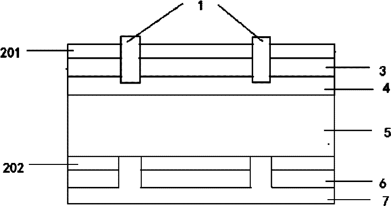
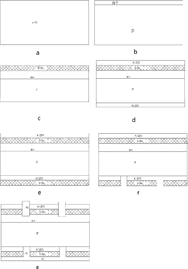
[0039] Steps §1, §2, §3, §5, §7 and §8 are all traditional crystalline silicon cell preparation processes, and the process parameters are different.

[0040] §1 figure 2 a, Use the general single crystal silicon cleaning method, that is, sodium hydroxide + isopropanol (NaOH + IPA) solution to remove the surface damage of P-type CZ silicon and make texture to form an anti-reflection structure and chemical cleaning; P-type CZ silicon wafer 125 monocrystalline silicon wafers for industrial use, resistivity 0.5-5Ωcm, thickness 180-220um;

[0041] §2 figure 2 b, Diffusion in a POCl3 atmosphere to form an n+ emitter and remove the surrounding pn junction and phosphosilicate glass to form a pn+ junction silicon substrate with a pn+ structure;

[0042] §3 figure 2 c, a 70nm amorphous silicon nitride film with a refractive index of 2.3 was deposited on the surface of the n+ emitter by conventional direct PECVD;

[0043] §4 Use HF acid to clean the surface of the structure obtain...


PUM

PropertyMeasurementUnit
thicknessaaaaaaaaaa
thicknessaaaaaaaaaa
thicknessaaaaaaaaaa

Abstract

The invention discloses a back point contact crystalline silicon solar cell and a preparation method thereof. The front surface of the solar cell is passivated by a silicon nitride/alumina double-layer film, the back surface of the solar cell is passivated by an alumina/silicon nitride double-layer film, and the back surface conducts current by point contact. The preparation method comprises the following steps: preparing the silicon nitride and the alumina, opening pores on the alumina/silicon nitride on the back surface, and removing an affected layer. The solar cell has the advantages of good surface passivation effect, good ultraviolet (UV) radiance resistance performance, high photoelectric conversion efficiency and the like, the back surface enhances internal reflection on the infrared light, and the front surface double-layer anti-reflection coating reduces surface reflection.

Description

technical field [0001] The invention relates to a crystalline silicon solar cell, in particular to a crystalline silicon solar cell with a double-layer passivation medium layer on the front surface and a back surface, point contact on the back surface and a preparation method thereof. Background technique [0002] In the production process of crystalline silicon solar cells, silicon nitride prepared by PECVD is used as the passivation layer and anti-reflection layer on the front surface. Passivation effect; literature reports that silicon nitride with a refractive index of 2.3 can achieve a surface recombination speed lower than 20cm / s. Considering the optimized combination of passivation and anti-reflection, industrial batteries generally use silicon nitride with a refractive index of about 2.0 and 80nm. Its passivation effect is not optimal. Screen printing paste is used and then sintered to prepare electrodes, especially silver paste is used on the back to prepare back e...

Claims


Application Information

Patent Timeline
Patent Type & Authority Applications(China)
IPC IPC(8): H01L31/052H01L31/0216H01L31/0224H01L31/18H01L31/056
CPCY02E10/52Y02E10/50Y02P70/50
Inventor 窦亚楠何悦王涛江作王建禄褚君浩
Owner SHANGHAI INST OF TECHNICAL PHYSICS - CHINESE ACAD OF SCI
Why Eureka
Try Eureka