Relaxation SiGe virtual substrate and preparation method thereof

A substrate and relaxation technology, used in semiconductor/solid-state device manufacturing, semiconductor devices, electrical components, etc., can solve the problems of complex process, large thickness of SiGe virtual substrate, rough surface, etc., to achieve low dislocation density, shorten the Epitaxy time, the effect of surface flattening

Inactive Publication Date: 2012-01-11
SHANGHAI INST OF CERAMIC CHEM & TECH CHINESE ACAD OF SCI
View PDF4 Cites 5 Cited by
  • Summary
  • Abstract
  • Description
  • Claims
  • Application Information

AI Technical Summary

Problems solved by technology

[0003] The purpose of the present invention is to provide a SiGe virtual substrate with a relaxed high germanium content and a preparation method thereof, so as to ove...

Method used


Image

  • Relaxation SiGe virtual substrate and preparation method thereof
  • Relaxation SiGe virtual substrate and preparation method thereof
  • Relaxation SiGe virtual substrate and preparation method thereof

Examples


Embodiment 1

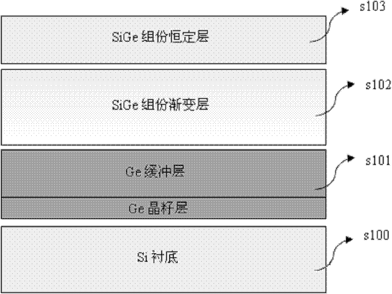
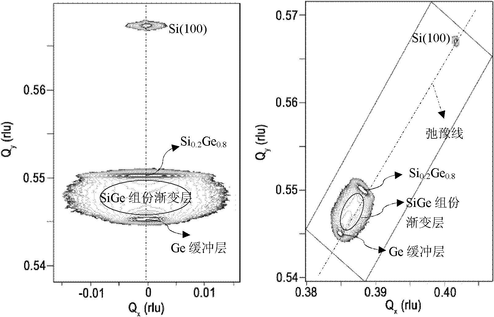
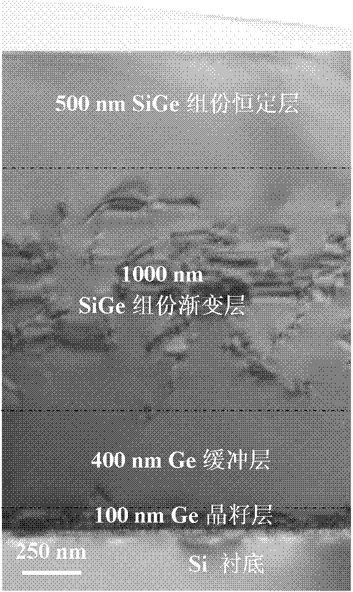
[0043] The preparation process of a SiGe dummy substrate with high germanium content is as follows: figure 1 shown to prepare Si 0.2 Ge 0.8 Taking the virtual substrate as an example, it includes the following steps:

[0044] In step s100, four 4-inch, 6-inch, 8-inch and 12-inch Si wafers are respectively prepared as Si substrates.

[0045] Step s101, growth of Ge relaxation buffer layer: based on 4-inch, 6-inch, 8-inch and 12-inch Si substrates, respectively, at 400 ° C with GeH 4 is the gas phase precursor, GeH 4 The flow rate is 150sccm, in H 2 As the carrier gas, the pressure in the growth chamber is 100Torr, and a Ge seed layer with a thickness of 50nm, 60nm, 100nm, and 100nm is deposited respectively; the growth atmosphere is kept constant, and then on the deposited four Ge seed layers at 700 Deposit Ge buffer layers with a thickness of 300nm, 340nm, 400nm and 600nm respectively at ℃, and anneal in situ (epitaxial growth chamber) at 850℃ for 10 minutes after complet...

Embodiment 2

[0054] A Si with high germanium content 0.15 Ge 0.85 The preparation of virtual substrate comprises the following steps:

[0055] In step s100, an 8-inch Si wafer is prepared as a Si substrate.

[0056] Step s101, growth of the Ge relaxation buffer layer: on the basis of an 8-inch Si substrate, at 350 ° C with GeH 4 is the gas phase precursor, GeH 4 The flow rate is 200sccm, in H 2 As the carrier gas, the growth chamber pressure is 100Torr, deposit a layer of Ge seed layer with a thickness of 100nm; keep the growth atmosphere unchanged, and then deposit a Ge buffer layer with a thickness of 400nm on the deposited Ge seed layer at 650°C, After completion, in-situ (epitaxial growth chamber) annealing at 850° C. for 10 minutes, maintaining the growth chamber pressure at 100 Torr during annealing, to obtain a Ge relaxation buffer layer with a thickness of 500 nm and complete strain relaxation.

[0057] Step s102, growth of a composition-graded SiGe buffer layer: on the basis ...

Embodiment 3

[0065] A Si with high germanium content 0.1 Ge 0.9 The preparation of virtual substrate comprises the following steps:

[0066] In step s100, a 6-inch Si wafer is prepared as a Si substrate.

[0067] Step s101, growth of the Ge relaxation buffer layer: on the basis of a 6-inch Si substrate, first at 400 ° C with GeH 4 is the gas phase precursor, GeH 4 The flow rate is 100sccm, in H 2 As the carrier gas, the growth chamber pressure is 50Torr, deposit a layer of Ge seed layer with a thickness of 100nm; keep the growth atmosphere unchanged, and then deposit a Ge buffer layer with a thickness of 500nm on the deposited Ge seed layer at 650°C, After completion, in-situ (epitaxial growth chamber) annealing at 800° C. for 10 minutes, while maintaining the pressure of the growth chamber at 100 Torr during annealing, obtained a Ge relaxation buffer layer with a thickness of 600 nm and complete strain relaxation.

[0068] Step s102, growth of a composition-graded SiGe buffer layer: ...


PUM

PropertyMeasurementUnit
Thicknessaaaaaaaaaa
Thicknessaaaaaaaaaa
Thicknessaaaaaaaaaa

Abstract

The invention belongs to the technical field of semiconductor materials, and relates to a relaxation SiGe virtual substrate with high Ge content and a preparation method thereof. The SiGe virtual substrate comprises a Si substrate, a Ge crystal seed layer, a Ge buffer layer, a SiGe buffer layer with variable components and a SiGe layer with constant components, wherein the Ge crystal seed layer, the Ge buffer layer, the SiGe buffer layer and the SiGe layer epitaxially grow on the Si substrate from inside to outside in sequence; and the Ge crystal seed layer and the Ge buffer layer form a Ge relaxation buffer layer. The SiGe virtual substrate has the characteristics of high Ge contents, complete relaxation, low dislocation density, thin thickness, smooth surface and the like. The preparation method of the SiGe virtual substrate is characterized in that the epitaxial layers grow on the Si substrate by adopting a decompression chemical vapor deposition method. The relaxation SiGe virtualsubstrate with high Ge content provided by the invention can be widely applied to Ge channel strain engineering and the preparation of high-mobility channel materials in a CMOS (complementary metal oxide semiconductor) technology, and the performances of a CMOS device are improved further.

Description

technical field [0001] The invention belongs to the technical field of semiconductor materials, and relates to a high-quality relaxed SiGe dummy substrate with high germanium content and a preparation method thereof. Background technique [0002] In the semiconductor industry, Si material has been developed as a dominant semiconductor device for nearly half a century. With the development of science and technology and people's pursuit of the performance of microelectronic devices, the feature size of semiconductor devices has been continuously reduced, and the size of a single transistor has gradually reached the dual limits of physics and technology. The performance of CMOS devices using traditional Si as the channel material It has been unable to meet the requirements of continuous improvement in the performance of semiconductor devices. People are stepping up the search for new methods and materials to maintain the pace of rapid growth of microelectronic devices. It is ...

Claims


Application Information

Patent Timeline
IPC IPC(8): H01L29/00H01L29/06H01L29/167H01L21/205
Inventor 刘学超陈之战施尔畏
Owner SHANGHAI INST OF CERAMIC CHEM & TECH CHINESE ACAD OF SCI
Why Eureka
Try Eureka