Solar panel preparing method
A technology of solar cells and silicon wafers, applied in circuits, electrical components, photovoltaic power generation, etc., can solve problems such as multiple impurities and micro-defects in solar cells, carrier recombination, and affecting photoelectric conversion efficiency of solar cells
- Summary
- Abstract
- Description
- Claims
- Application Information
AI Technical Summary
Problems solved by technology
Method used
Image
Examples
preparation example Construction
[0015] The invention provides a method for preparing a solar cell, the steps comprising:
[0016] a, preparing a-Si:H thin film on the surface of the silicon wafer after texturing;
[0017] b. Treating the silicon wafer containing the a-Si:H film on the surface obtained in step a at a high temperature of 800-900° C. for 60-120 min;
[0018] c. Etching the surface of the high temperature treated silicon wafer.
[0019] It can be combined with phosphorus diffusion treatment, and the front side of the silicon wafer deposited with a-Si:H film can be treated with phosphorus diffusion at the same time of high temperature treatment. In this case, the thickness of the a-Si:H film deposited on the back and front of the silicon wafer Different, the thickness of the a-Si:H film deposited on the front side is generally thinner, which is made into an oxide layer, and then phosphorus diffusion treatment is performed to prepare a perfect PN junction. It is preferable to remove the gettered...
Embodiment 1
[0030] Gettering and Diffusion Processes in the Preparation of Solar Cells
[0031] a) Using plasma enhanced chemical vapor deposition (PECVD), SiH 4 and H 2 For the reactive gas, SiH 4 and H 2 Plasma occurs under the action of microwaves, and then reacts to form a-Si:H film on the back surface of the textured silicon wafer. The substrate temperature is 400°C, the microwave power is 3000W, the power frequency is 2.45GHz, and the reaction gas SiH 4 :H 2 =1:10, the deposition time is 200s, and the thickness of a-Si:H film is: 100nm.
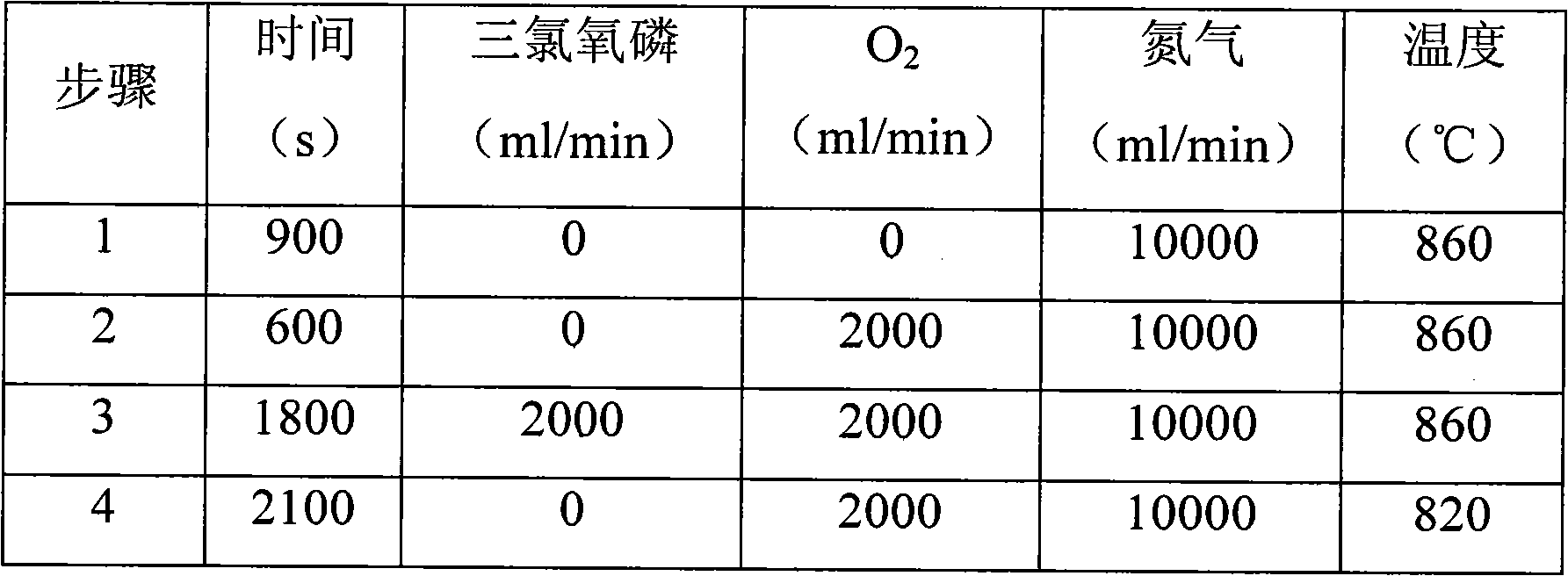
[0032] b) Insert the above-mentioned crystalline silicon wafers with a-Si:H thin film back-to-back into a quartz boat, and put them into a diffusion furnace (TS81254 model produced by Tempress Company) to carry out phosphorus diffusion and gettering, the time and temperature of each step of the process And the amount of each gas flow is shown in the table below:
[0033]
[0034] c) Use the back chemical etching to make the silicon wafer ...
Embodiment 2
[0036] Gettering and Diffusion Processes in the Preparation of Solar Cells
[0037] a) Using plasma enhanced chemical vapor deposition (PECVD), SiH4 and H 2 For the reactive gas, SiH 4 and H 2 Plasma occurs under the action of microwaves, and then reacts to form a-Si:H film on the back surface of the textured silicon wafer. The substrate temperature is 400°C, the microwave power is 3000W, the power frequency is 2.45GHz, and the reaction gas SiH 4 :H 2 =1:10, the deposition time is 200s, and the thickness of a-Si:H film is: 100nm.
[0038] b) Put the crystalline silicon wafer with the a-Si:H thin film deposited on the backside into a high-temperature furnace and process at 860° C. for 90 minutes.
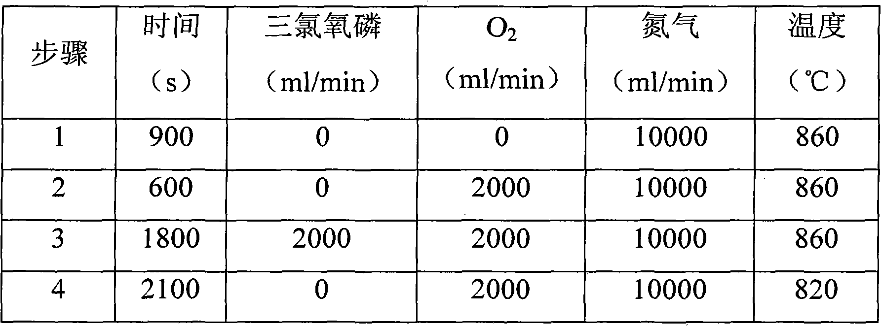
[0039] Finally, put the crystalline silicon wafer with the a-Si:H thin film deposited on the back after the high temperature treatment into the diffusion furnace for phosphorus diffusion process. The time, temperature and the amount of various gases in each step of this process ...
PUM
| Property | Measurement | Unit |
|---|---|---|
| thickness | aaaaa | aaaaa |
| thickness | aaaaa | aaaaa |
Abstract
Description
Claims
Application Information


