Circuit board having multicycle planar electromagnetic band gap structure

A technology of electromagnetic bandgap and electromagnetic bandgap unit, which is applied in the direction of printed circuit components, etc., can solve problems such as limiting the scope of application, achieve good signal integrity, reduce impact, and suppress synchronous switching noise.

Inactive Publication Date: 2012-01-11
XIDIAN UNIV
View PDF2 Cites 12 Cited by
  • Summary
  • Abstract
  • Description
  • Claims
  • Application Information

AI Technical Summary

Problems solved by technology

The power layer plane of these planar electromagnetic bandgap structures often adopts a single-period unit structure, and its bandgap width only depends on the equivalent inductance and equivalent capacitance of the bridge connection between adjacent structural units, among which I-bridge type...

Method used


Image

  • Circuit board having multicycle planar electromagnetic band gap structure
  • Circuit board having multicycle planar electromagnetic band gap structure
  • Circuit board having multicycle planar electromagnetic band gap structure

Examples


Embodiment Construction

[0024] The present invention will be described in further detail below with reference to the accompanying drawings.

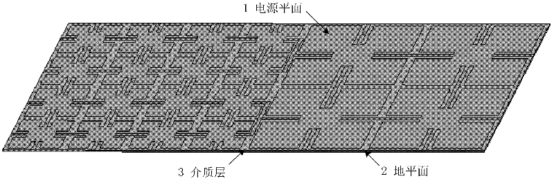
[0025] refer to figure 1 , The circuit board of the present invention is mainly composed of a power plane 1 , a ground plane 2 and a dielectric layer 3 . The power plane 1 is located on the top layer of the circuit board of the present invention, and it adopts such as figure 2 The multi-period planar electromagnetic bandgap structure shown is used to suppress synchronous switching noise; the ground plane 2 is located at the bottom of the circuit board of the present invention, and a complete metal plane is used to provide a return path for signals; the dielectric layer 3 is located on the power plane Between 1 and ground plane 2, FR4 dielectric material with a thickness of 0.4mm and a relative permittivity of 4.4 is used to isolate the power plane 1 and ground plane 2;

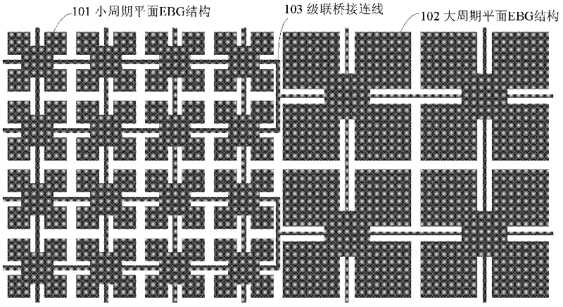
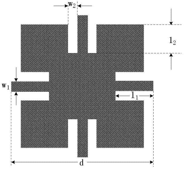
[0026] refer to figure 2 , the power supply plane 1 of the circuit board of the presen...


PUM

PropertyMeasurementUnit
Thicknessaaaaaaaaaa

Abstract

The invention discloses a circuit board having a multicycle planar electromagnetic band gap structure. According to the invention, a problem ofnarrow stop band width of a current circuit board with a planar electromagnetic band gap is solved. The circuit board provided in the invention is composed of a power source plane (1), a ground plane (2), and a dielectric layer (3). The power source plane (1) comprises a plurality of minor cycle planar electromagnetic band gap units (101), a plurality of major cycle planar electromagnetic band gap units (102) and a plurality of cascading bridging line connections (103); the two planar electromagnetic band gap units (101) and (102) are respectively at a left side and a right side of the power source plane and are arranged in a square matrix mode; besides, the two planar electromagnetic band gap units are connected by the cascading bridging line connections (103) to construct a multicycle power source planar structure. According to the invention, when an inhibition depth is -30 dB, a stop band range is from 0.7 GHz to 8.4 GHz and a stop band width is 7.7 GHz; compared with a circuit board having a single cycle planar electromagnetic band gap unit, the circuit board provided in the invention has an obviously broadened band gap width, so that synchronous switch noise can be effectively inhibited; therefore, the circuit board provided in the invention can be applied to a high speed circuit and a broadband device.

Description

technical field [0001] The invention belongs to the technical field of electronic devices, relates to a planar electromagnetic bandgap structure, and can be directly applied to suppress synchronous switching noise in a wide frequency range in high-speed circuits. Background technique [0002] With the development of modern CMOS technology, especially the increase of system clock frequency and pulse edge slew rate, and the reduction of power supply voltage and noise margin, how to suppress the synchronous switching noise on the power or ground plane, that is, ground bounce noise, It has become a major challenge in high-speed circuit design. Over the past decade, researchers have tried various methods to suppress synchronous switching noise to maintain a noise-free power distribution system, the most typical of which is the use of decoupling capacitors. However, when the system operates at high frequencies, this method is no longer effective due to the inherent wire inductanc...

Claims


Application Information

Patent Timeline
IPC IPC(8): H05K1/02
Inventor 来新泉史凌峰张颖肖垣明毕明路
Owner XIDIAN UNIV
Why Eureka
Try Eureka