Method for growing nanocrystalline silicon powder

A technology of nanocrystalline silicon and powder, which is applied in the field of preparation of nanocrystalline silicon powder, can solve the problems of poor plasma stability, insufficient decomposition of raw material gas, unsuitable for large-scale industrial production, etc. Low equipment cost and uniform discharge effect

Inactive Publication Date: 2012-01-18
HEBEI UNIVERSITY
View PDF3 Cites 11 Cited by
  • Summary
  • Abstract
  • Description
  • Claims
  • Application Information

AI Technical Summary

Problems solved by technology

[0005] The document "L.Mangolini, E.Thimsen, U.Kortshagen. High-Yield Plasma Synthesis of Luminescent Silicon Nanocrystals, NANO LETTERS, 2005, 5(4): 655-659." discloses a method based on plasma-enhanced chemical vapor deposition A method and device for preparing nanocrystalline silicon powder, using a jet flow device to generate dielectric barrier discharge plasma, wherein a copper ring serving as an electrode is placed on the ventilation pipe, and the raw material gas passes through the plasma formed by electrification from top to bottom In the area, the gas decomposes and grows into nanocrystalline silicon particles, and then collects them on the lower collecting net. The plasma generated by this method has poor stability, the raw material gas cannot be fully decomposed, and the uniformity of the generated nanocrystalline silicon powder cannot be guaranteed. That is, the size of nanocrystalline silicon particles cannot be precisely controlled, so it is not suitable for large-scale industrial production

Method used


Image

  • Method for growing nanocrystalline silicon powder
  • Method for growing nanocrystalline silicon powder
  • Method for growing nanocrystalline silicon powder

Examples


Embodiment Construction

[0031] The present invention will be further described in detail below in conjunction with the accompanying drawings and specific embodiments.

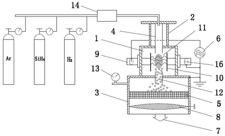
[0032] A method for growing nanocrystalline silicon powder, the key of which is to comprise the following steps:

[0033] A. Pass the mixed gas from the inlet pipe 2 into the reaction chamber 1, the flow ratio is: argon 30-150sccm, silane 0.8-1.3sccm, hydrogen 1-10sccm, wherein, argon is the working gas, silane hydrogen is the reaction gas;

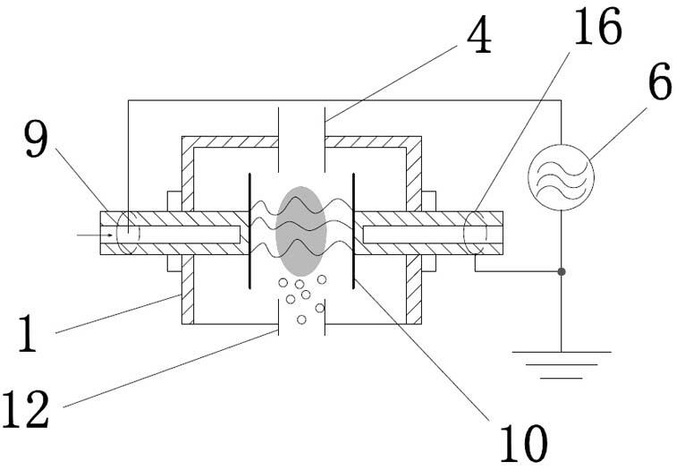
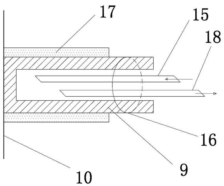
[0034] B. Input radio frequency alternating current into a pair of horizontally arranged electrodes 9 through radio frequency source 6, so that the working gas is discharged, and a plasma region 11 is formed between the quartz plates 10 as electrode barrier layers;

[0035] C. The reaction gas is decomposed by plasma in the plasma region 11, and the decomposed fragments form nanocrystalline silicon nuclei;

[0036] D, adjust the flow rate L of the gas that passes through flowmeter 14 and / or adj...


PUM


Abstract

The invention discloses a method for growing nanocrystalline silicon powder. The method comprises the following steps: introducing gas mixture into a reaction chamber from gas inlet pipelines; inputting radio frequency alternating current into electrodes which are vertically arranged by a radio frequency source to cause working gases to discharge to form a plasma zone between quartz plates; enabling reactive gases to be decomposed by plasmas in the plasma zone, and enabling fragments obtained after decomposition to form nanocrystalline silicon cores; controlling the time spent on flowing through the plasma zone by the reactive gases by adjusting the flow of the introduced gases and/or adjusting the pressure of the reaction chamber, and controlling the sizes of the grown nanocrystalline silicon particles by controlling the retention time; and enabling the nanocrystalline silicon particles to stop growing after flowing out of the plasma zone along with airflow, and carrying out collection on a connection net to obtain the nanocrystalline silicon powder with uniformly distributed particle sizes. The method disclosed by the invention is simple to operate, has lower requirements for temperature, dispenses with heating devices, can be used for producing nanocrystalline silicon powder with uniformly distributed and controllable particle sizes, and can realize industrial production.

Description

technical field [0001] The invention relates to a method for preparing nanocrystalline silicon powder, in particular to a method for continuously growing monodisperse nanocrystalline silicon powder by using plasma generated by radio frequency dielectric barrier discharge. Background technique [0002] Due to the quantum confinement effect of nanostructures, silicon nanostructure materials exhibit a wide range of energy level tunability and room temperature luminescence characteristics, and are widely used in optoelectronic devices, full-color displays, solar cells, bioluminescent labels, optical communications, and silicon-based optical integration. It has great application potential. [0003] At present, a variety of technologies have been applied to the preparation of nano-sized nanocrystalline silicon powder. The commonly used preparation methods mainly include chemical vapor deposition, sol-gel method, chemical solution precipitation method, pulsed laser ablation method,...

Claims


Application Information

Patent Timeline
Patent Type & Authority Applications(China)
IPC IPC(8): C01B33/03B82Y40/00
Inventor 于威徐艳梅王新占詹小舟傅广生
Owner HEBEI UNIVERSITY
Why Eureka
Try Eureka