Novel substrate, epitaxial wafer and semiconductor device
An epitaxial wafer and semiconductor technology, applied in semiconductor devices, electrical components, circuits, etc., can solve the problems of reducing the resistance uniformity of the epitaxial layer, low resistivity uniformity, and difficulty in reducing the resistivity uniformity value. Steep, reduce production cost, improve product quality effect
- Summary
- Abstract
- Description
- Claims
- Application Information
AI Technical Summary
Problems solved by technology
Method used
Image

Examples
Embodiment 1-4
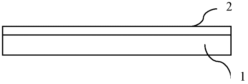
[0033] Such as figure 2 As shown, the novel substrate includes a substrate body 1 with a single crystal silicon layer 2 on the surface of the substrate body 1 . The thickness of the single crystal silicon layer 2 is 2-5 μm. Its specific thickness can be determined according to the overall thickness of the epitaxial wafer and the thickness of the substrate body. The higher the substrate thickness, the thicker the monocrystalline silicon layer. In subsequent production, an epitaxial layer is grown on the surface of the single crystal silicon layer 2 .
[0034] The substrate body 1 can be N-type, that is, doped with arsenic, phosphorus or antimony; the substrate body 1 can also be P-type, that is, doped with boron.
[0035] Examples 1-4 are all heavy arsenic-doped substrate bodies, and in Examples 1-4, 2 μm, 2.6 μm, 3.5 μm, and 4.8 μm single crystal silicon layers are respectively arranged between the substrate body and the epitaxial layer.
[0036] In Examples 1-4, the mono...
Embodiment 5-8
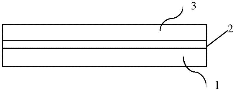
[0038] image 3 It is a schematic diagram of the epitaxial wafer structure in Embodiment 5-8. Examples 5-8 used the substrates in Examples 1-4, respectively. Such as image 3 As shown, an epitaxial layer 3 is formed on the surface of the single crystal silicon layer 2 . The monocrystalline silicon layer 2 is located between the substrate body 1 and the epitaxial layer 3 .
[0039] In Comparative Examples 1-4, the substrate body is heavily doped with arsenic, and no single crystal silicon layer is provided between the substrate body and the epitaxial layer.
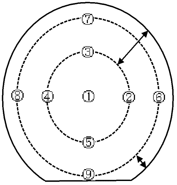
[0040] The comparative data of the epitaxial layer resistance uniformity of Examples 5-8 and Comparative Examples 1-4 are shown in Table 1-4. In each group of comparisons, two substrate bodies produced in the same batch were selected, one was provided with a single crystal silicon layer and then grown an epitaxial layer; the other was directly grown with an epitaxial layer. The epitaxial layer growth process is the sa...
Embodiment 9
[0052]Two heavy phosphorus-doped substrate bodies produced in the same batch were selected, one was used in Example 9, and an epitaxial layer 3 was grown after growing a monocrystalline silicon layer 2 on the surface of the substrate body 1; the other was used in Comparative Example 5, The epitaxial layer is directly grown on the surface of the substrate body. The single crystal silicon layer 2 in Example 9 is formed by reacting trichlorosilane with hydrogen. The reaction temperature was 960° C., and the hydrogen flow rate was 140 slm / s. The single crystal silicon produced by the reaction is deposited on the surface of the substrate body 1 to form a single crystal silicon layer 2 . The single crystal silicon layer 2 has a thickness of 4 μm.
[0053] In Comparative Example 5, no single crystal silicon layer is provided between the substrate body and the epitaxial layer.
[0054] The epitaxial layer growth process in Example 9 and Comparative Example 5 is the same.
[0055] ...
PUM
| Property | Measurement | Unit |
|---|---|---|
| Thickness | aaaaa | aaaaa |
| Thickness | aaaaa | aaaaa |
| Thickness | aaaaa | aaaaa |
Abstract
Description
Claims
Application Information