Asymmetrical multichip system level integrated packaging device and packaging method for same

A technology of integrated packaging and packaging methods, which is applied in the manufacture of semiconductor devices, electrical solid state devices, semiconductor/solid state devices, etc., can solve the problems of high aspect ratio and cost, and achieve the effects of high frequency integration, low RC delay, and wide application range

Inactive Publication Date: 2012-04-04
SHANGHAI XINCHU INTEGRATED CIRCUIT
View PDF3 Cites 10 Cited by
  • Summary
  • Abstract
  • Description
  • Claims
  • Application Information

AI Technical Summary

Problems solved by technology

This penetrating silicon channel (TSV technology) ensures high-density RC delay wiring through the shortest line length, but the aspect ratio of TSV technology is also high, such as figure 2

Method used


Image

  • Asymmetrical multichip system level integrated packaging device and packaging method for same
  • Asymmetrical multichip system level integrated packaging device and packaging method for same
  • Asymmetrical multichip system level integrated packaging device and packaging method for same

Examples


Embodiment Construction

[0032] The present invention will be described in detail below in conjunction with the accompanying drawings.

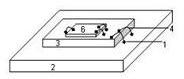
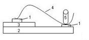
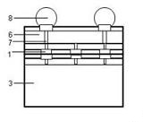
[0033] In the drawings: 1 pad, 2 substrate, 3 bottom chip, 4 connection wire, 5 bonding head, 6 top chip, 7 penetrating silicon channel, 8 solder ball, 9 spacer barrier layer, 10 metal line in chip, 11 Plasma generator, 12 plasma vent ring, 13 vacuum cover, 14 failure pad, 15 redundant repair pad, 16 redundant repair metal layer, 17 transistor, 18 polymer, 19 small pad, 20 vacuum pressure welding suction head, 21-wafer mobile platform.

[0034] image 3 , Figure 4 It is a structural schematic diagram of an embodiment of the present invention. Including: pad 1, such as CU, substrate, such as PCB 2, bottom chip 3, connection wire 4, such as AL, top chip 6, and metal wire 10 in the chip. Through the face-to-face contact between the top chip and the bottom chip, the pads 1 of the top chip and the bottom chip are bonded, and the bottom chip is connected to the substrat...


PUM


Abstract

The invention discloses an asymmetrical multichip system level integrated packaging device, which comprises a top chip, a bottom chip, a substrate and connecting wires, wherein the substrate is placed below the bottom chip, the dimension of the top chip is smaller than that of the bottom chip, connecting pads or connecting soldering flux bumps are arranged on the bottom chip, a pad face of the top chip is arranged downwardly, a pad face of the bottom chip is arranged upwardly, the bottom chip is placed on the substrate, the pads of the top chip and the top chip are in face-to-face bonding, and the bottom chip is connected with the substrate through the connecting wires. The invention further discloses a packaging method for the asymmetrical multichip system level integrated packaging device. The asymmetrical multichip system level integrated packaging device is low in cost and has the advantages of high density, high frequency and low signal RC (resistance-capacitance) delay.

Description

technical field [0001] The invention specifically relates to an asymmetric multi-chip system-level integrated package device and a package method thereof. Background technique [0002] Although through the integration of standard logic processes between systems and processes such as embedded dynamic random access memory or embedded flash memory or embedded radio frequency or embedded sensors, it is possible to realize high-bandwidth interconnection and interconnection with low signal RC delay, and quickly improve the mask Stencil count, however, low yields and high fab costs are several factors that have reconsidered packaged system packages from 2D to 3D high-density packages. Chip-to-chip packaging from vertically stacked wafer levels to flip-chip top die and bottom die. The high cost of system chips such as embedded dynamic random access memory, embedded flash memory, embedded radio frequency and embedded sensors has led international major manufacturers in this technolo...

Claims


Application Information

Patent Timeline
Patent Type & Authority Applications(China)
IPC IPC(8): H01L25/16H01L23/498H01L21/68H01L21/98
CPCH01L2224/85181H01L2224/48091H01L2224/48472H01L2224/73265H01L24/80H01L24/08H01L24/48H01L24/73H01L25/0657H01L2224/08121H01L2224/80895H01L2224/80896H01L2224/8014H01L2224/80139H01L2224/80013H01L2224/8009H01L2224/75745H01L2224/73201H01L23/66H01L2223/6611H01L2225/0651H01L2225/06524H01L2225/06527H01L2225/06572H01L2224/08145H01L2924/00014H01L2924/00H01L2224/08H01L2224/48
Inventor 陈邦明
Owner SHANGHAI XINCHU INTEGRATED CIRCUIT
Why Eureka
Try Eureka