Monolithic integration processing method for unequal-height silicon structure and integrated circuit

A technology of integrated circuits and processing methods, applied in the field of single-chip integrated processing of high-silicon structures and integrated circuits, which can solve problems affecting device performance and achieve the effect of ensuring performance

Inactive Publication Date: 2012-05-02
PEKING UNIV
View PDF6 Cites 6 Cited by
  • Summary
  • Abstract
  • Description
  • Claims
  • Application Information

AI Technical Summary

Problems solved by technology

However, in this processing method, when using silicon isotropic etching to realize the air isolation groove, the device structure will also be etched laterally. At the same time, the floating electrodes composed of dielectric materials such as silicon oxide and metals have relatively large stress. The MEMS structure is not All composed of single crystal silicon, which affects the performance of the device

Method used


Image

  • Monolithic integration processing method for unequal-height silicon structure and integrated circuit
  • Monolithic integration processing method for unequal-height silicon structure and integrated circuit
  • Monolithic integration processing method for unequal-height silicon structure and integrated circuit

Examples


Embodiment Construction

[0023] The present invention will be described in detail below in conjunction with the accompanying drawings and embodiments.

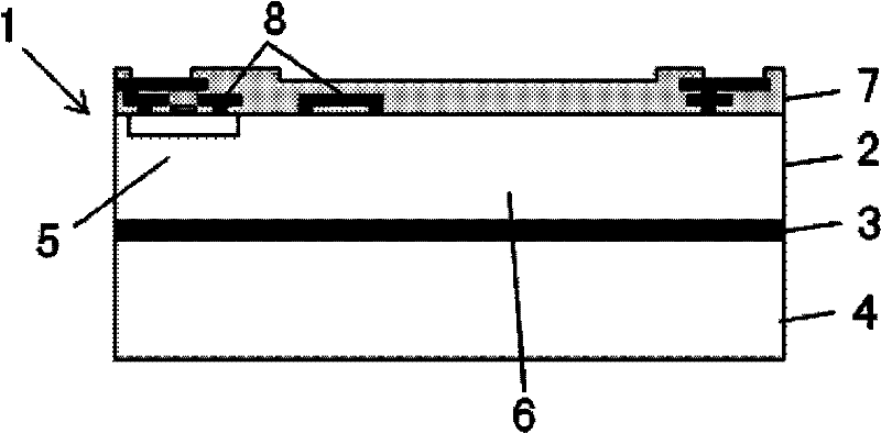
[0024] Such as figure 1 Shown, the present invention adopts and realizes integrated circuit processing on SOI (Silicon-on-insulator silicon on insulator) substrate, and it comprises the steps:

[0025] 1) select SOI substrate 1, SOI substrate 1 includes device layer 2, buried oxide layer 3 and substrate layer 4, wherein, device layer 2 is made of integrated circuit region 5 and MEMS (micro-electromechanical system) structure region 6; Wherein, The silicon structure corresponding to the integrated circuit region 5 and the silicon structure corresponding to the MEMS structure region 6 are mechanically connected through the buried oxide layer 3 and the substrate layer 4 .

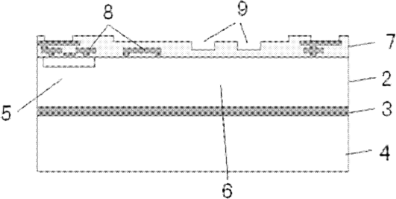
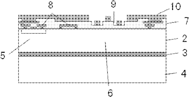
[0026] 2) Integrated circuit processing is carried out on the integrated circuit area 5 of the SOI substrate 1, and a dielectric layer 7 of silicon oxide or silicon nitride is genera...


PUM


Abstract

The invention relates to a monolithic integration processing method for an unequal-height silicon structure and an integrated circuit. The method comprises the following steps of: (1) selecting a silicon-on-insulator (SOI) substrate comprising a device layer, a buried oxygen layer and a substrate layer; (2) processing the integrated circuit on the device layer, and generating a medium layer; (3) etching the medium layer for the first time to form a medium layer shallow slot, and manufacturing a mask area of which the height is reduced; (4) making a photoresist graphic corresponding to a microelectromechanical system (MEMS) structural mask area; (5) etching the medium layer until the device layer is manufactured into an MEMS structural mask; (6) performing first-time silicon anisotropic etching on the device layer by using the MEMS structural mask without penetration of the device layer; (7) removing a height reduction structural mask by an anisotropic reaction ion etching method, and thinning a standard structural mask; (8) performing second-time silicon anisotropic etching until an unequal-height MEMS silicon structure of the buried oxygen layer is obtained; (9) manufacturing an isolation groove on the device layer; and (10) removing the substrate layer and the buried oxygen layer which correspond to the unequal-height MEMS silicon structure to finish processing an unequal-height MEMS device. The method can be widely applied in the fields of processing of MEMSs.

Description

technical field [0001] The invention relates to a monolithic integrated processing method of a silicon structure and an integrated circuit, in particular to a monolithic integrated processing method of a unequal-height silicon structure and an integrated circuit in the field of micro-electromechanical systems (MEMS). Background technique [0002] MEMS (Microelectromechanical Systems) refers to the use of a manufacturing process compatible with the integrated circuit (IC) process to realize a micro-integrated system that integrates information acquisition, information storage, information processing and execution. It has low cost, small size, Light weight, low power consumption and other advantages. Making the signal processing circuit and the MEMS mechanical structure on the same chip to achieve single chip integration will greatly reduce the volume, weight and power consumption of the entire system, and improve the reliability of the system. More importantly, the integrati...

Claims


Application Information

Patent Timeline
Patent Type & Authority Applications(China)
IPC IPC(8): B81C1/00B81B7/00
Inventor 杨振川闫桂珍郝一龙
Owner PEKING UNIV
Why Eureka
Try Eureka