Capacitive type micro-acceleration sensor with double-sided symmetrical elastic beam structure and manufacturing method
A technology of acceleration sensor and elastic beam, which is applied in the field of micro-electromechanical systems, can solve the problems of complex process and high cost, and achieve the effects of simplified process, stable performance and improved process controllability
- Summary
- Abstract
- Description
- Claims
- Application Information
AI Technical Summary
Problems solved by technology
Method used
Image
Examples
Embodiment 1
[0057] 1. Fabrication of elastic beam-mass structure:
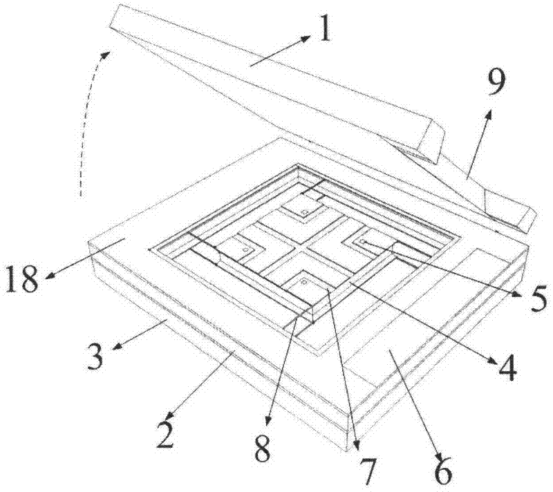
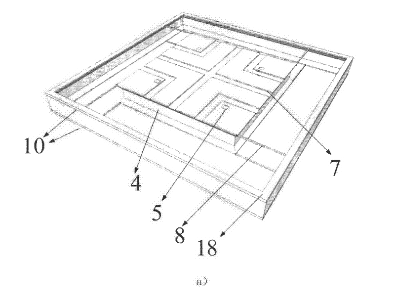
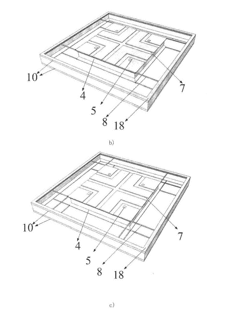
[0058] (1) Utilize the anisotropic etching method to make a capacitor gap 12 on the upper and lower surfaces of the oxidized double-throwing double-device layer SOI silicon wafer, and the etching depth is 1 μm ( image 3 b);
[0059] (2) Remove the oxide layer in the remaining area, perform secondary oxidation to form silicon oxide, double-sided photolithography, and make overload protection bumps 5 (1 μm in height) on the upper and lower surfaces of the mass block by anisotropic etching method, such as image 3 c;
[0060] (3) Remove the oxide layer in the remaining area, oxidize to form silicon oxide, use double-sided photolithography, and use anisotropic etching method to etch a double-sided symmetrical elastic beam-mass structure pattern on the upper and lower surfaces of the silicon wafer, etch The stop layer is the buried oxide layer of SOI, and forms the damping adjustment groove 7, such as image 3 d; Width of ...
Embodiment 2
[0070] The manufacturing method of the damping adjustment groove in the first embodiment is as follows: by designing the width of the damping groove, anisotropic corrosion is used to self-stop to form a V-shaped damping adjustment groove. In Example 2, a two-step photolithography method is used to fabricate the damping adjustment groove.
[0071] (1) Utilize the anisotropic etching method to make a capacitor gap 12 on the upper and lower surfaces of the oxidized double-throwing double-device layer SOI silicon wafer, and the etching depth is 1 μm, such as Figure 4 as shown in a;
[0072] (2) Remove the oxide layer in the remaining area, form silicon oxide by secondary oxidation, double-sided photolithography, and make overload protection bumps (1 μm in height) on the upper and lower surfaces of the mass block by anisotropic etching method, such as Figure 4 as shown in b;
[0073] (3) Remove the oxide layer in the remaining area, oxidize to form silicon oxide, use double-sid...
PUM
 Abstract
Description
Claims
Application Information


