Pd-Ni/SiNWs array electrode glucose sensor and manufacturing method and application thereof

A glucose sensor and array electrode technology, which is applied in the field of glucose detection, can solve the problems of sensor incompatibility, etc., and achieve the effects of increased detection sensitivity, mature technology, and simple operation methods

Inactive Publication Date: 2012-07-04
EAST CHINA NORMAL UNIV
View PDF2 Cites 4 Cited by
  • Summary
  • Abstract
  • Description
  • Claims
  • Application Information

AI Technical Summary

Problems solved by technology

There have been reports on metal-modified carbon nanotubes and metal-modified carbon nanobelts as glucose sensors. However, such sensors are not compatible with integrated circuits, and silicon nanomaterials are well compatible with integrated circuit technology.
Although it has been reported in the literature that Au and Mg modified silicon nanowires (SiNWs) are used as the detection material for glucose, and palladium nickel is modified on the surface of silicon nanowires by electroless co-deposition technology to produce highly sensitive, high-selective and unaffected by interferences. Glucose sensors are rarely reported in the patent literature

Method used


Image

  • Pd-Ni/SiNWs array electrode glucose sensor and manufacturing method and application thereof
  • Pd-Ni/SiNWs array electrode glucose sensor and manufacturing method and application thereof
  • Pd-Ni/SiNWs array electrode glucose sensor and manufacturing method and application thereof

Examples


preparation example Construction

[0032] The preparation method of the Pd-Ni / SiNWs array electrode glucose sensor in this embodiment, the specific steps include:

[0033] Step 1: using the silicon substrate material 1 as the silicon substrate material for growing the SiNWs array, and growing the base SiNWs array material layer 2 by chemical wet etching;

[0034] Step 2: On the substrate SiNWs array material layer 2, a metal Pd-Ni nanoparticle coating 3 is provided, and the metal Pd-Ni nanoparticle coating 3 is modified by electroless plating technology to obtain a Pd-Ni / SiNWs array material;

[0035] Step 3: performing rapid thermal annealing on the Pd-Ni / SiNWs array material prepared in step 2 under the protection of nitrogen atmosphere;

[0036] Step 4: Bond the copper wire 6 to the surface of the Pd-Ni / SiNWs array material with silver paste and connect it to the metal Pd-Ni nanoparticle coating 3 to form a Pd-Ni / SiNWs array electrode, and place it in a drying oven to dry;

[0037] Step 5: Wrap the silv...

Embodiment 1

[0039] 1. Preparation of silicon nanowires (SiNWs) materials by chemical wet etching

[0040] (1) Use P-type (100) crystal orientation (resistivity: 1~10 ) Double-sided polished silicon wafers, cut into 0.5×0.5cm samples, cleaned by standard RCA process, put into 35mM / L silver nitrate (AgNO 3 ) and a mixed etching solution composed of 20% hydrofluoric acid HF to grow SiNWs, and the etching time is about 40 minutes.

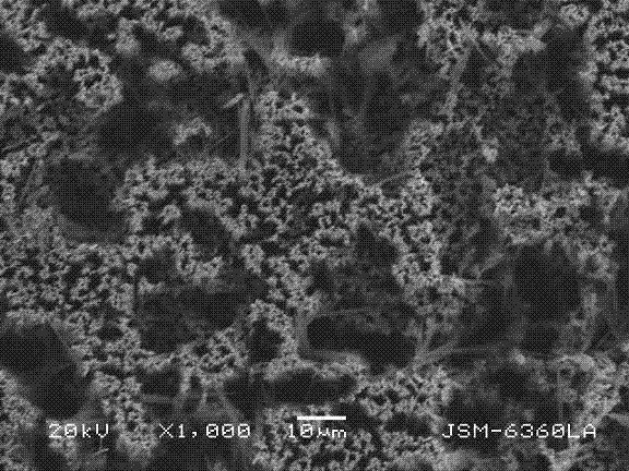
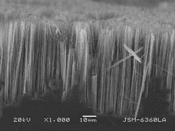
[0041] (2) Wash away the remaining silver particles on the etched SiNWs surface with 65% nitric acid solution by mass percentage, clean the SiNWs surface with a large amount of deionized water, and dry it in an oven at 80 °C. The surface morphology of the prepared SiNWs is as follows figure 1 and 2 as shown, figure 1 Shown is the SEM top view of SiNWs; figure 2 Shown is the SEM profile of SiNWs. The diameter of SiNWs is about 200nm, and the length is about 50-60μm.

[0042] 2. Electroless plating technology to modify metal Pd-Ni on the surface of silicon ...

Embodiment 2

[0052] The parts that are the same as those in Embodiment 1 will not be described again.

[0053] 1. Fabrication of Silicon Nanowires (SiNWs) by Chemical Wet Etching

[0054] (1) Use P-type (100) crystal orientation (resistivity: 1-10 ) Double-sided polished silicon wafers, cut into 0.5cm×0.5cm samples, cleaned by standard RCA process, put in 30mM / L silver nitrate AgNO 3 In a mixed etching solution composed of 20% by mass of hydrofluoric acid HF, silicon nanowires were grown, and the etching time was 50 minutes.

[0055] (2) Wash away the remaining silver particles on the etched SiNWs surface with a nitric acid solution with a mass percentage of 30%, and clean the SiNWs surface with a large amount of deionized water, and then dry it in an oven at 80 °C. The prepared SiNWs have a diameter of about 150 nm and a length of 70 μm to 90 μm.

[0056] 2. Electroless plating technology modified metal palladium nickel on the surface of silicon nanowires to make Pd-Ni / SiNWs arra...


PUM

PropertyMeasurementUnit
diameteraaaaaaaaaa
lengthaaaaaaaaaa

Abstract

The invention discloses Pd-Ni / SiNWs array electrode glucose sensor which comprises silicon substrate material, a basal SiNWs array material layer, a metal Pd-Ni nanoparticle coated layer, a copper wire and an epoxy resin protection layer. The basal SiNWs array material layer is grown on the silicon substrate material; the metal Pd-Ni nanoparticle coated layer is arranged on the basal SiNWs array material layer; the copper wire is arranged on the metal Pd-Ni nanoparticle coated layer,; and the epoxy resin protection layer wraps the contact part of the copper wire and the metal Pd-Ni nanoparticle coated layer. The invention further discloses a manufacturing method and application of the Pd-Ni / SiNWs array electrode glucose sensor. The Pd-Ni / SiNWs array electrode glucose sensor has a small volume, a large surface area, high activity, high sensitivity and interference resistance and can be applied widely.

Description

technical field [0001] The invention relates to the technical field of glucose detection, in particular to a Pd-Ni / SiNWs array electrode glucose sensor and a preparation method and application thereof. Background technique [0002] Glucose detection technology is a detection technology that is closely related to human life, and has a wide range of applications in biotechnology, clinical medicine and food analysis. Most of the traditional glucose sensors use oxidase electrodes as identification and signal conversion devices. However, the development of such glucose sensors is limited because the enzyme activity is easily affected by time, temperature, pH, humidity, and poisoning effects of compounds. Therefore, people began to study the glucose sensor without enzyme structure. This type of sensor has good stability, simple manufacturing process, high repeatability and low cost, and what is more valuable is that it is not easily affected by the oxygen concentration in the so...

Claims


Application Information

Patent Timeline
Patent Type & Authority Applications(China)
IPC IPC(8): G01N27/26
Inventor 张健回士超严强陈雪皎任旭
Owner EAST CHINA NORMAL UNIV
Why Eureka
Try Eureka