

Manufacturing method of quantum point contact
A quantum dot contact and contact technology, applied in the field of nanotechnology research and storage, can solve the problems of demanding instruments, narrow material selection range, harsh conditions, etc., and achieve high preparation precision, wide application range and simple preparation process. Effect
- Summary
- Abstract
- Description
- Claims
- Application Information
AI Technical Summary
Problems solved by technology
Method used
Image

Examples
Embodiment 1
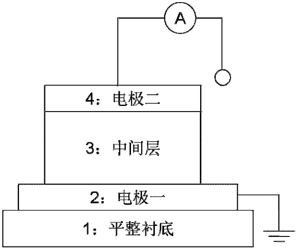
[0039] In this embodiment, the "sandwich" structural unit (such as figure 1 Shown) the electrode one 2 adopts the platinum that thickness is 10~200 nanometers, preferably about 100 nanometers, and the intermediate layer 3 adopts the zinc oxide that thickness is 10~200 nanometers, preferably about 100 nanometers, and electrode two 4 adopts the thickness and is 10 nanometers. ~200 nm, preferably about 100 nm of niobium.
[0040] The above-mentioned "sandwich" structural unit can be prepared sequentially on a flat substrate by using the existing coating process, and one of the preparation methods is as follows:
[0041] Step 1. First, sputtering a layer of metal platinum electrode as electrode 1 on the flat substrate cleaned by ultrasonic cleaning with acetone and ethanol in advance by means of electron beam evaporation;
[0042] Step 2, place the flat substrate 1 grown with electrode 1 in a high vacuum environment, use magnetron sputtering in an atmosphere with an argon-oxygen ...
Embodiment 2
[0047] In this embodiment, the "sandwich" structural unit (such as figure 1 As shown), the electrode one 2 adopts indium tin oxide with a thickness of 10-200 nanometers, preferably about 100 nanometers, the intermediate layer 3 adopts zinc oxide with a thickness of 10-200 nanometers, preferably about 100 nanometers, and the electrode two 4 adopts Indium tin oxide with a thickness of 10-200 nanometers, preferably about 100 nanometers.
[0048] The above-mentioned "sandwich" structural unit can be prepared sequentially on a flat substrate by using the existing coating process, and one of the preparation methods is as follows:
[0049] Step 1. Firstly, sputtering a layer of metal indium tin oxide electrode as electrode-2 on the clean flat substrate after ultrasonic cleaning with acetone and ethanol in advance;
[0050] Step 2, place the flat substrate 1 grown with electrode 1 in a high vacuum environment, use magnetron sputtering in an atmosphere with an argon-oxygen pressure ra...
Embodiment 3
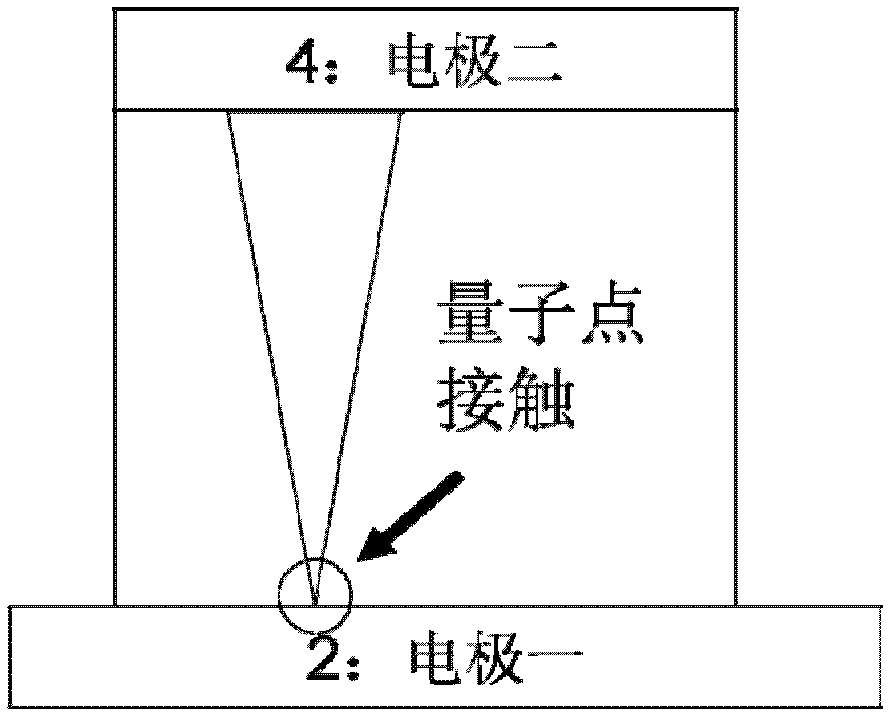
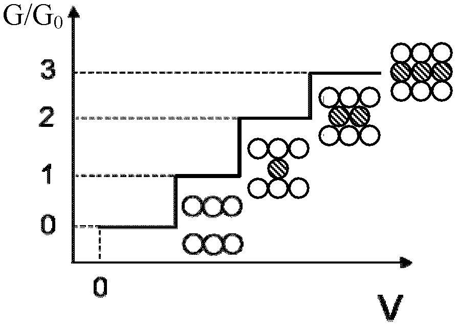
[0054] In this embodiment, the method for preparing the quantum dot contact is basically the same as that of Embodiment 1, the difference is that electrode 2 adopts platinum with a thickness of 10 to 200 nanometers, preferably about 100 nanometers, and the intermediate layer 3 adopts platinum with a thickness of 10 to 200 nanometers. nanometer, preferably about 200 nanometers of zinc oxide, and the second electrode 4 is copper with a thickness of 10-200 nanometers, preferably about 100 nanometers. Similarly, when a voltage is applied to both ends of the electrode 2 and the electrode 4, the ions and / or vacancies in the conductive region 2 formed by the electrode 2 and the intermediate layer are moved to the conductive region 1 formed by the electrode 2 under the driving of the electric field. A conductive channel is formed between regions; by adjusting the voltage amplitude, the conductance G of the conductive channel reaches NG 0 , where N is a natural number, G 0 In order to...
PUM
| Property | Measurement | Unit |
|---|---|---|
| Thickness | aaaaa | aaaaa |
| Conductance value | aaaaa | aaaaa |
| Conductance value | aaaaa | aaaaa |
Abstract
Description
Claims
Application Information