

Nitride light-emitting device for improving light-emitting efficiency by electron barrier layer
A technology of electron blocking layer and light-emitting device, which is applied in the direction of electrical components, semiconductor devices, circuits, etc., can solve problems such as unfavorable light fields, and achieve the effects of overcoming parasitic quantum well phenomenon, uniform light gain, and high luminous intensity
- Summary
- Abstract
- Description
- Claims
- Application Information
AI Technical Summary
Problems solved by technology
Method used
Image

Examples
Embodiment 1
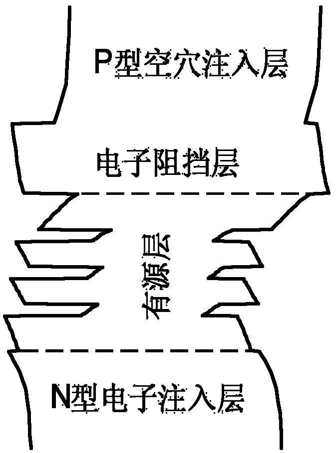
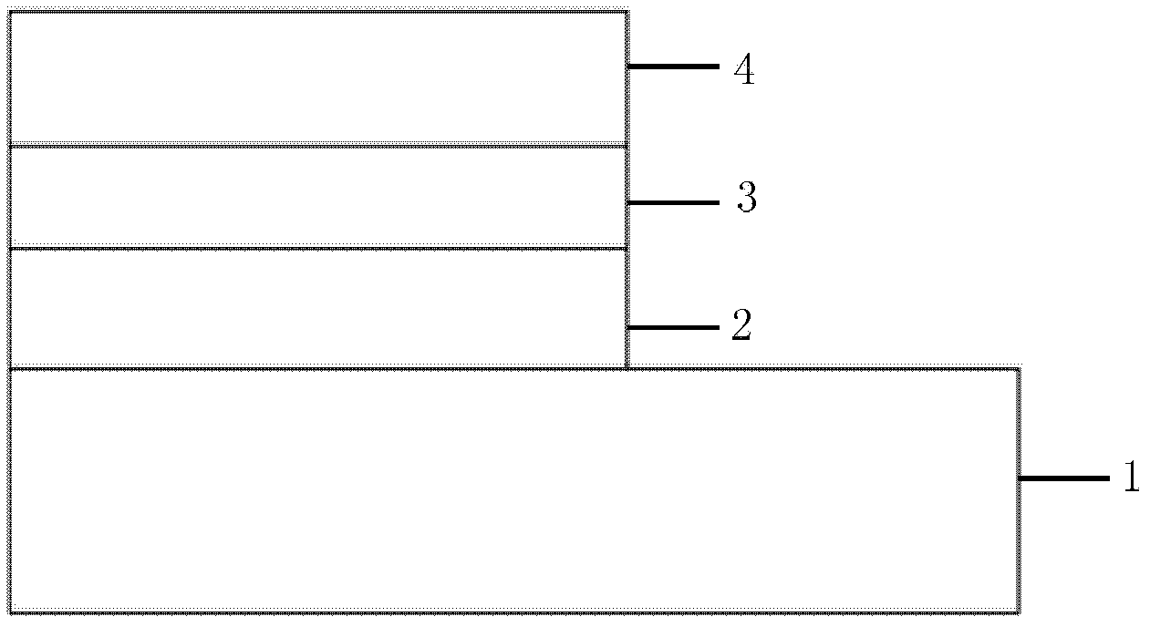
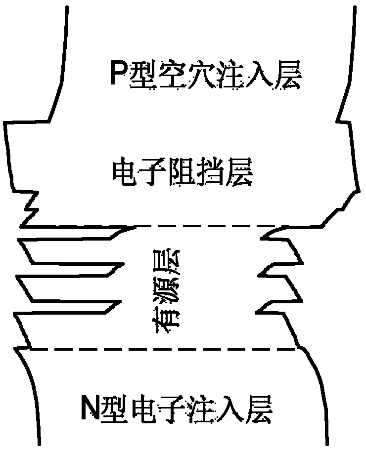
[0022] Such as figure 2 As shown, in this embodiment, the nitride light-emitting device adopts a nitride laser, including four parts stacked sequentially from the substrate to the top: a multi-layered N-type electron injection layer 1, an active layer 2, an electron blocking layer 3, and a P-type hole injection layer 4 with a multilayer structure.
[0023] The N-type electron injection layer of multilayer structure includes N-type contact layer, N-type cladding layer and N-type waveguide layer; the active layer includes quantum wells and quantum barriers; the P-type hole injection layer of multilayer structure includes P-type waveguide layer, P-type cladding layer and P-type contact layer.
[0024] The contact layer, cladding layer and waveguide layer can be one of binary system nitrides such as AlN, InN and GaN, or one of ternary system nitrides such as AlGaN, InAlN and InGaN, or even AlInGaN One of the quaternary nitrides.
[0025] Wherein, the electron blocking layer in...
Embodiment 2
[0030] The structure of the light-emitting device is the same as in Embodiment 1, wherein the electron blocking layer includes two layers of AlGaN, and the composition (atomic number) of Al is linearly interpolated and gradually changed, wherein the composition of the first layer of Al is gradually changed from 0 to 0.05, and the composition of the second layer is gradually changed from 0 to 0.05. The composition of Al is gradually changed from 0.06 to 0.35, and the thicknesses of the first layer and the second layer of AlGaN are 5nm and 25nm respectively.
[0031] Each of the three AlGaN layers of the electron blocking layer is P-type uniformly Mg doped.
[0032] Embodiment 2 is an electron blocking layer structure with gradually changing Al composition, and the composition of Al in the two layers from bottom to top is increased by linear interpolation.
[0033] The power-current curves of the light-emitting devices of the prior art, embodiment 1 and embodiment 2 are summariz...
PUM
 Abstract
Description
Claims
Application Information