Preparation method of small-size density-controllable silicon nanodot array

A technology of silicon nano and dot arrays, which is applied in the field of preparation of small-sized density thyristor nano dot arrays by electrochemical etching, and achieves good application prospects, uniform size distribution, and controllable nano dot size and density

Inactive Publication Date: 2012-07-11
XIAMEN UNIV
View PDF4 Cites 2 Cited by
  • Summary
  • Abstract
  • Description
  • Claims
  • Application Information

AI Technical Summary

Problems solved by technology

[0036] The purpose of the present invention is to provide a method for preparing a small-sized density thyristor nano-dot...

Method used


Image

  • Preparation method of small-size density-controllable silicon nanodot array
  • Preparation method of small-size density-controllable silicon nanodot array
  • Preparation method of small-size density-controllable silicon nanodot array

Examples


Embodiment 1

[0059] (1) Depositing an aluminum film on a silicon wafer: Deposit an aluminum film with a thickness of 1 μm on a single crystal silicon by magnetron sputtering.

[0060] (2) Annealing: anneal the silicon wafer after the aluminum film is deposited in a nitrogen atmosphere at 350° C. for 6 h to increase the grain size of the deposited aluminum film and improve the bonding degree between it and the substrate.

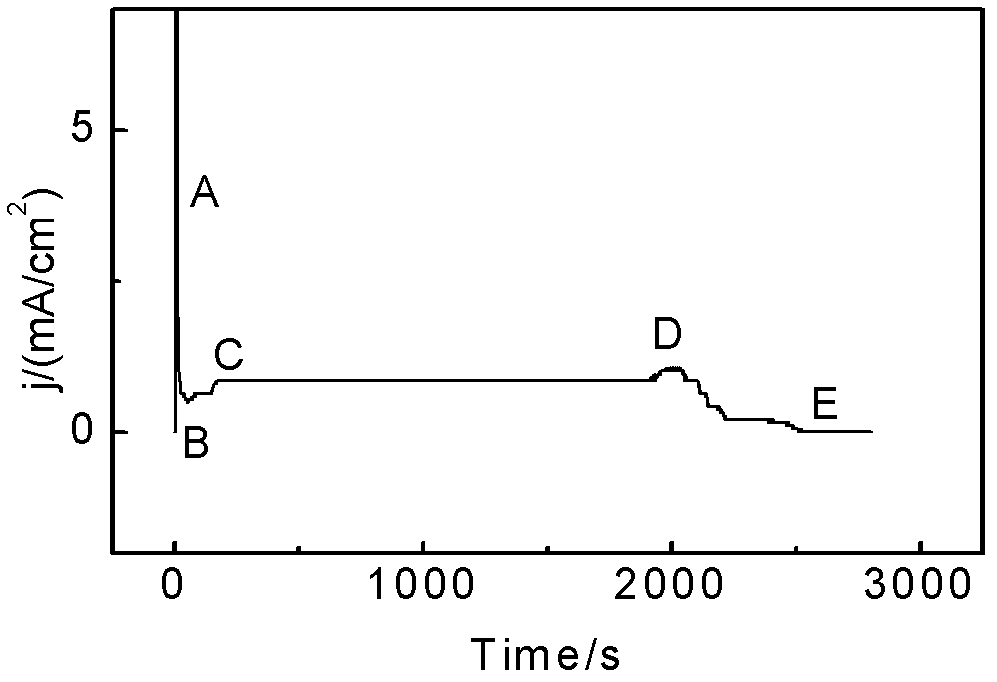
[0061] (3) Carrying out anodic oxidation on the aluminum film: in 15wt% sulfuric acid, the oxidation is carried out at a voltage of 20V. Oxidation proceeds to stop at point E. figure 1 A typical current density / time curve of the anodic oxidation process on a silicon substrate is given, where point E represents the complete end of oxidation, and any time after point E can be selected to stop the oxidation process.

[0062] (4) Remove the anodic aluminum oxide film formed in step 3 and the silicon dioxide spots on the surface of the silicon substrate: use 6% phosphoric aci...

Embodiment 2

[0065] (1) Depositing an aluminum film on a silicon wafer: an aluminum film with a thickness of 1.5 μm is deposited on a single crystal silicon by electron beam evaporation.

[0066] (2) Annealing: anneal the silicon wafer after the aluminum film is deposited in a nitrogen atmosphere at 450° C. for 4 hours to increase the grain size of the deposited aluminum film and improve the bonding degree between it and the substrate.

[0067] (3) Anodizing the aluminum film: in 0.3M oxalic acid, oxidize at a voltage of 40V. Oxidation proceeds to stop at point E.

[0068] (4) Remove the anodic aluminum oxide film formed in step 3 and the silicon dioxide spots on the surface of the silicon substrate: use 6% phosphoric acid to remove the anodic aluminum oxide film in a water bath at 30° C. for 5 hours, and then use 1% hydrofluoric acid Soak the sample in acid for 5 min to remove silicon dioxide spots on the surface of the silicon substrate. The samples were then removed and exposed to air...

Embodiment 3

[0071] (1) Depositing an aluminum film on a silicon wafer: Deposit an aluminum film with a thickness of 2 μm on a single crystal silicon using thermal evaporation equipment.

[0072] (2) Annealing: anneal the silicon wafer after the aluminum film is deposited in a nitrogen atmosphere at 550° C. for 2 h to increase the grain size of the deposited aluminum film and improve the bonding degree between it and the substrate.

[0073] (3) Anodizing the aluminum film: oxidizing at a voltage of 60V in 0.3M sulfuric acid. Oxidation proceeds to stop at point E.

[0074] (4) Remove the anodic aluminum oxide film formed in step 3 and the silicon dioxide spots on the surface of the silicon substrate: use 6% phosphoric acid to remove the anodic aluminum oxide film in a 40°C water bath for 5 hours, and then use 5% hydrofluoric acid Soak the sample in acid for 5 min to remove silicon dioxide spots on the surface of the silicon substrate. The samples were then removed and exposed to air.

[...


PUM


Abstract

The invention discloses a preparation method of a small-size density-controllable silicon nanodot array, relating to a preparation method of the silicon nanodot array. The preparation method comprises the following steps of: depositing an aluminum film on a substrate, then annealing and anodizing the aluminum film; removing silica dots on the surfaces of the formed anodized aluminum film and the silicon substrate, namely, forming a silicon nanodot array with larger size on the surface of a sample; and deoxidizing the sample to obtain the large-area, uniform, small-size density-controllable silicon nanodot array without an insulated barrier layer. The prepared silicon nanodots are uniform in size distribution and controllable in size and density; and no insulated layer exists between the silicon nanodots and the substrate, so that preparation of electric/photoelectric components is facilitated; meanwhile, the preparation method disclosed by the invention is simple in process conditions and free of complex equipment and has favorable application prospect in large-scale industrial production.

Description

technical field [0001] The invention relates to a method for preparing a silicon nano-dot array, in particular to a method for preparing a silicon-controlled nano-dot array with a small size and density by an electrochemical etching method. Background technique [0002] In the early 1990s, Canham et al. [1,2] Si or SiGe nanostructures prepared by electrochemical anodic corrosion (mainly composed of nanostructures with a diameter less than 5nm [2] ), a strong visible emission was observed at room temperature. This finding has aroused great interest in the luminescence of Si-based nanostructures. [0003] In the past 20 years, great progress has been made in the preparation methods of Si-based nanostructures. At present, the common preparation methods of Si-based nanostructures are as follows: [0004] (1) Laser Ablation Deposition (PLD) [0005] Laser ablation deposition uses a focused pulsed laser beam with a certain wavelength and energy density to irradiate a single c...

Claims


Application Information

Patent Timeline
IPC IPC(8): H01L21/02
Inventor 黄凯李阳娟李成赖虹凯
Owner XIAMEN UNIV
Why Eureka
Try Eureka