High-power intracavity frequency-doubled semiconductor disk laser

A thin-film laser, intra-cavity frequency doubling technology, applied in semiconductor lasers, lasers, laser parts, etc., can solve the problems of high laser threshold, large scattering loss, and inability to emit light, achieve spectral brightness enhancement, increase output power, improve The effect of heat dissipation

Inactive Publication Date: 2012-07-11
BEIJING UNIV OF TECH
View PDF3 Cites 13 Cited by
  • Summary
  • Abstract
  • Description
  • Claims
  • Application Information

AI Technical Summary

Problems solved by technology

The heat dissipation of the SDL can be partially improved by etching the substrate of the semiconductor gain sheet, but this technology has extremely high requirements on the process, because in this technology, the semiconductor gain medium is grown in reverse order, and the final etching surface is the light output surface, the finish must be very good, otherwise it will cause excessive scattering loss due to the rough surface, resulting in too high threshold and low efficiency of the laser, or even no light output at all.

Method used


Image

  • High-power intracavity frequency-doubled semiconductor disk laser
  • High-power intracavity frequency-doubled semiconductor disk laser
  • High-power intracavity frequency-doubled semiconductor disk laser

Examples


Embodiment 1

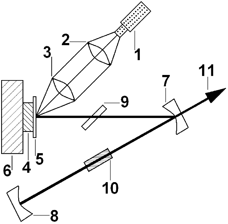
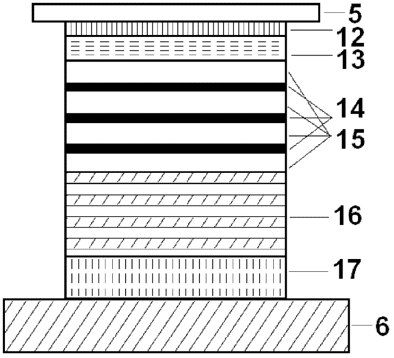
[0026] Such as figure 1 As shown, an 808nm semiconductor laser pumping light source 1 passes through a collimator lens 2 with a focal length of 10 mm, and then is focused on a semiconductor sheet gain medium 4 by a focusing lens 3 with the same focal length as the collimator lens 2 . The structure of semiconductor thin gain medium is as follows figure 2 As shown, the uppermost anti-oxidation protective layer 12 is GaAs, and the lower high barrier carrier confinement layer 13 is AlGaAs, wherein the Al content is 0.6, and the carrier confinement layer is a multi-quantum well periodic gain structure, wherein The semiconductor quantum well layer 14 is InGaAs, the In content is 0.198, the quantum well barrier layer 15 is AlGaAs, the Al content is 0.05, the bottom is the Bragg reflector 16, and its high refractive index layer is GaAs, and the low refractive index layer is AlAs , the entire semiconductor thin slice gain medium is grown on the GaAs substrate 17, and then welded on t...

Embodiment 2

[0028] The semiconductor laser pumping light source 1 is 670nm; the semiconductor quantum well layer in the semiconductor sheet gain medium is GaAs, the quantum well barrier layer is AlGaAs, and the Al content is 0.2; the Bragg mirror is composed of GaAs / AlAs periods, and the number of periods is 25 -35; the rear reflector is highly reflectively coated for the 850nm and 425nm bands, the output coupling mirror is highly reflectively coated for the 850nm band, and is highly transparently coated for the 425nm band; the filter device 9 is an uncoated glass etalon with a thickness of 40 μm; The linear crystal adopts a 10mm long LBO frequency-doubling crystal cut for 850nm fundamental frequency light, and both ends of the crystal are coated with an anti-reflection coating for 850nm; it can obtain high-power frequency-doubling blue light output in the 425nm band.

Embodiment 3

[0030] Such as Figure 5 As shown, on the basis of Embodiment 1, the output coupling mirror 7 is plated with high-reflection coatings in three bands of 1064nm, 532nm and 355nm, and the rear end mirror 8 is tilted to make it a folded mirror, that is, a mirror 18, and a pair of 1064nm and 355nm bands are added. The reflection mirror 20 with 532nm high-reflection coating and 355nm transmittance forms another sub-cavity. In this sub-cavity, the triple frequency nonlinear crystal LBO, that is, the nonlinear crystal 19, can be placed in the optical waist to obtain the ultraviolet light in the 355nm band. Laser output.


PUM


Abstract

The invention relates to a high-power intracavity frequency-doubled semiconductor disk laser, which belongs to the technical field of semiconductor lasers. According to the invention, the heating effect of the laser is improved by using a heat-dissipating window, the frequency of fundamental-frequency lasers is stabilized and the line width of fundamental-frequency lasers is narrowed by using a filtering device, thereby improving the intracavity frequency-doubled efficiency. A pumping light subjected to collimating and focusing acts on a semiconductor disk gain medium (4), and a high-heat-conductivity heat-dissipating window (5) which is transparent to the pumping light and laser is bonded on the semiconductor disk gain medium; a photon-generated carrier in the gain medium has stimulated radiation in a quantum well (14), a laser cavity consisting of a rear-end mirror (8), an output coupling mirror (7), and a Bragg mirror (16) at the bottom of the semiconductor disk gain medium generates fundamental-frequency lasers, and a nonlinear crystal (10) generates frequency-doubled lasers (11); and the semiconductor disk laser is characterized in that: a filtering device (9) is arranged in the laser cavity, so that the frequency of fundamental-frequency lasers is stabilized effectively, and the line width of the fundamental-frequency lasers is narrowed many times, thereby improving the frequency-doubled efficiency.

Description

technical field [0001] The invention relates to the design of a high-power intracavity frequency-doubling semiconductor thin-sheet laser with a heat dissipation window and a filtering device, and belongs to the technical field of semiconductor lasers. Background technique [0002] Semiconductor Disk Laser (SDL) combines the advantages of both semiconductor lasers and solid-state disk lasers. On the one hand, SDL has the advantages of semiconductor lasers: the wavelength covers a wide range from visible light to near-infrared; the semiconductor absorbs the interband transition of pumping light so that its absorption bandwidth is very wide, and it is not sensitive to the wavelength shift of pumping light; the device It has high efficiency, long life and small size. On the other hand, SDL has the advantages of solid-state thin-plate lasers: the beam quality is very good, and a circular TEM near the diffraction limit can be obtained. 00 Gaussian mode; optical pumping can produ...

Claims


Application Information

Patent Timeline
Patent Type & Authority Applications(China)
IPC IPC(8): H01S5/024H01S5/06H01S5/10
Inventor 宋晏蓉张鹏张晓于振华田金荣
Owner BEIJING UNIV OF TECH
Why Eureka
Try Eureka