Non-equilibrium junction terminal structure for super-junction device

A technology of super junction devices and junction terminals, which is applied in semiconductor devices, electrical components, circuits, etc., can solve the problems that P columns cannot be completely depleted, cannot be completely ionized, and the electric field strength is small, so as to improve the breakdown voltage characteristics and overall The effect of reducing the device area and reducing the on-resistance

Active Publication Date: 2012-09-26
XIAN LONTEN RENEWABLE ENERGY TECH +1
View PDF3 Cites 10 Cited by
  • Summary
  • Abstract
  • Description
  • Claims
  • Application Information

AI Technical Summary

Problems solved by technology

[0005] In the voltage-resistant layer of the cell region of the superjunction device, the number of ions in the P-column and N-column regions is basically equal to maintain charge balance, but in the junction terminal region, the electric field strength is smaller than that of the cell region, so that th

Method used


Image

  • Non-equilibrium junction terminal structure for super-junction device
  • Non-equilibrium junction terminal structure for super-junction device
  • Non-equilibrium junction terminal structure for super-junction device

Examples


Embodiment

[0027] A MOSFET having a superjunction structure is illustrated, but the present invention is not limited to MOSFETs.

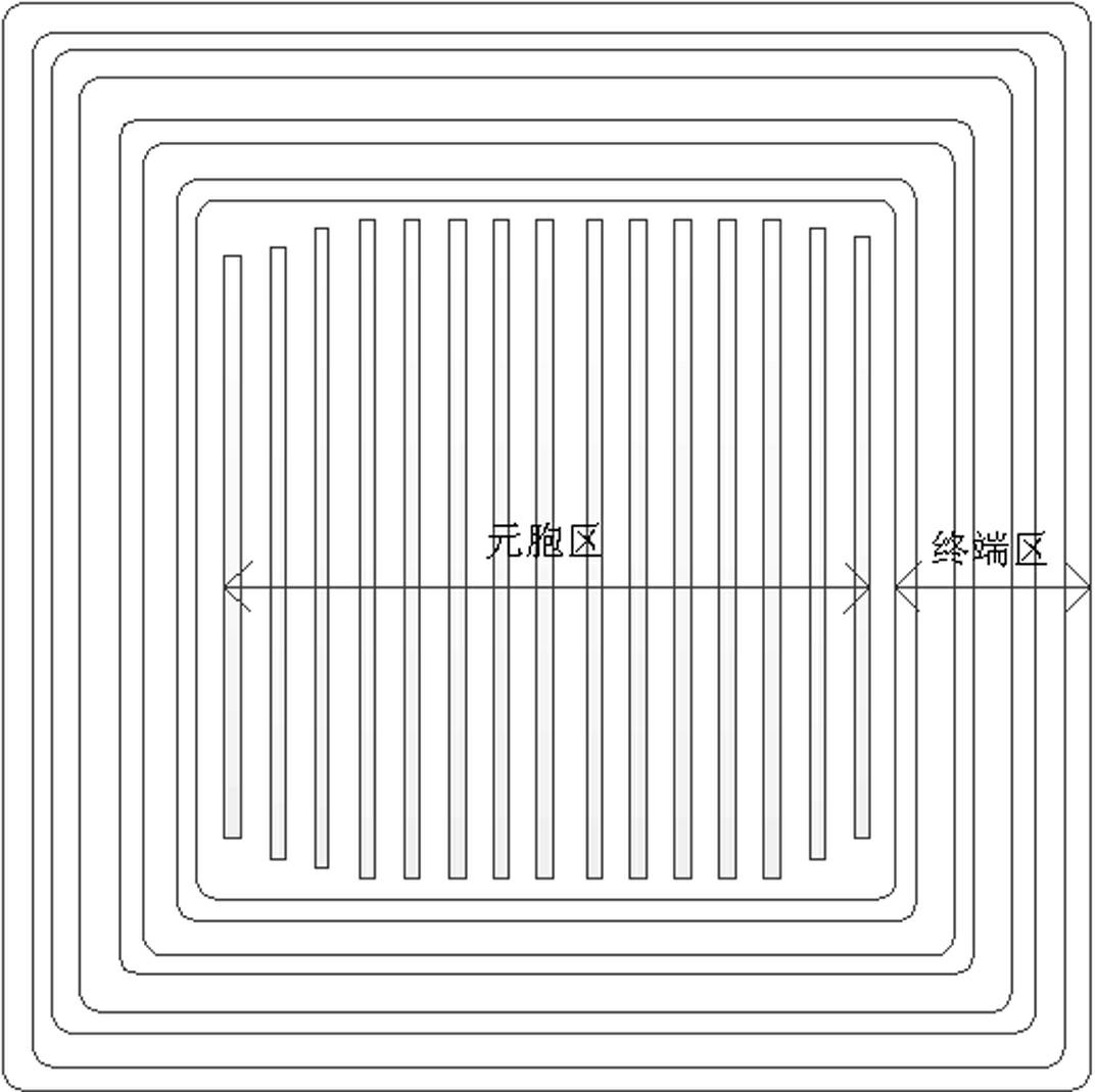
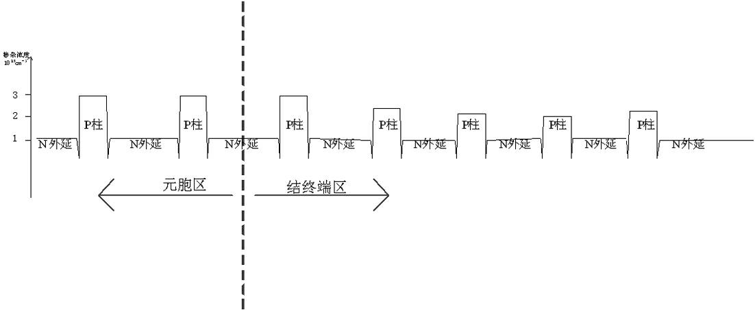
[0028] 1. N with a resistivity of 0.001Ω??cm + A 9 μm N epitaxial layer is grown on a silicon wafer substrate, and then a P-pillar mask is used to mask high-energy boron ion implantation. This is repeated four times, and a high-temperature and long-term pushing junction is performed to form a continuous P-pillar, and the N epitaxial layer Typical doping concentration is 1×10 15 cm -3 , the typical doping concentration of the P-column in the cell area is 3×10 15 cm -3 .

[0029] 2. Form a 900nm-thick field oxide layer by means of dry oxygen plus wet oxygen plus dry oxygen, and perform etching to form an active region.

[0030] 3. Dry oxygen to grow a gate oxide layer with a thickness of 100nm, then deposit polysilicon with a thickness of 400nm, and etch the polysilicon to form a polysilicon gate electrode and a polysilicon field plate structure.

[0031]...


PUM


Abstract

The invention relates to a non-equilibrium junction terminal architecture for a super-junction device. The junction terminal region of the terminal structure is provided with a plurality of uniform P pillars with different doping concentrations; the effective ion implantation area of the P pillars is correspondingly adjusted on the layout design according to the transverse electric field distribution conditions of all positions, so that the P pillars are completely exhausted when achieving the breakdown voltage; the ions are simultaneously implanted into all the P pillars under the masking of the mask sheet, thereby controlling the total amount of acceptor ions of all the P pillars in the junction terminal region; and after carrying out multiple extensions and multiple ion implantation processes, long-time high-temperature junction push is carried out to form several uniform P pillars with different doping concentrations. The invention can effectively improve the breakdown voltage characteristics of the junction terminal device, and has smaller junction terminal length, so that the total area of the device is reduced, thereby reducing the device conduction resistance on the same chip area.

Description

technical field [0001] The invention belongs to the field of semiconductor devices and process manufacturing, and in particular relates to an unbalanced junction terminal structure of a super junction device. Background technique [0002] Super junction VDMOS is a new type of power semiconductor device with rapid development and wide application. It introduces a superjunction (Superjunction) structure on the basis of ordinary vertical double-diffused metal oxide semiconductor (VDMOS), so that it has VDMOS high input impedance, fast switching speed, high operating frequency, voltage control, good thermal stability, and drive The circuit is simple, and overcomes the shortcoming that the on-resistance of VDMOS and the breakdown voltage increase sharply in the relationship of 2.5 powers. At present, super-junction VDMOS has been widely used in power supplies or adapters of consumer electronics products such as computers, mobile phones, lighting, LCD or plasma TVs and game conso...

Claims


Application Information

Patent Timeline
IPC IPC(8): H01L29/78H01L29/06
Inventor 姜贯军
Owner XIAN LONTEN RENEWABLE ENERGY TECH
Why Eureka
Try Eureka