Bragg reflection waveguide double-beam laser and application method thereof
A Bragg reflection and laser technology, used in semiconductor lasers, lasers, laser parts and other directions, can solve the problems of difficult to stabilize device output power, complex optical alignment, difficult mass production, etc., to achieve compactness and high stability, Large laser cavity, the effect of improving reliability
- Summary
- Abstract
- Description
- Claims
- Application Information
AI Technical Summary
Problems solved by technology
Method used
Image
Examples
Embodiment 1
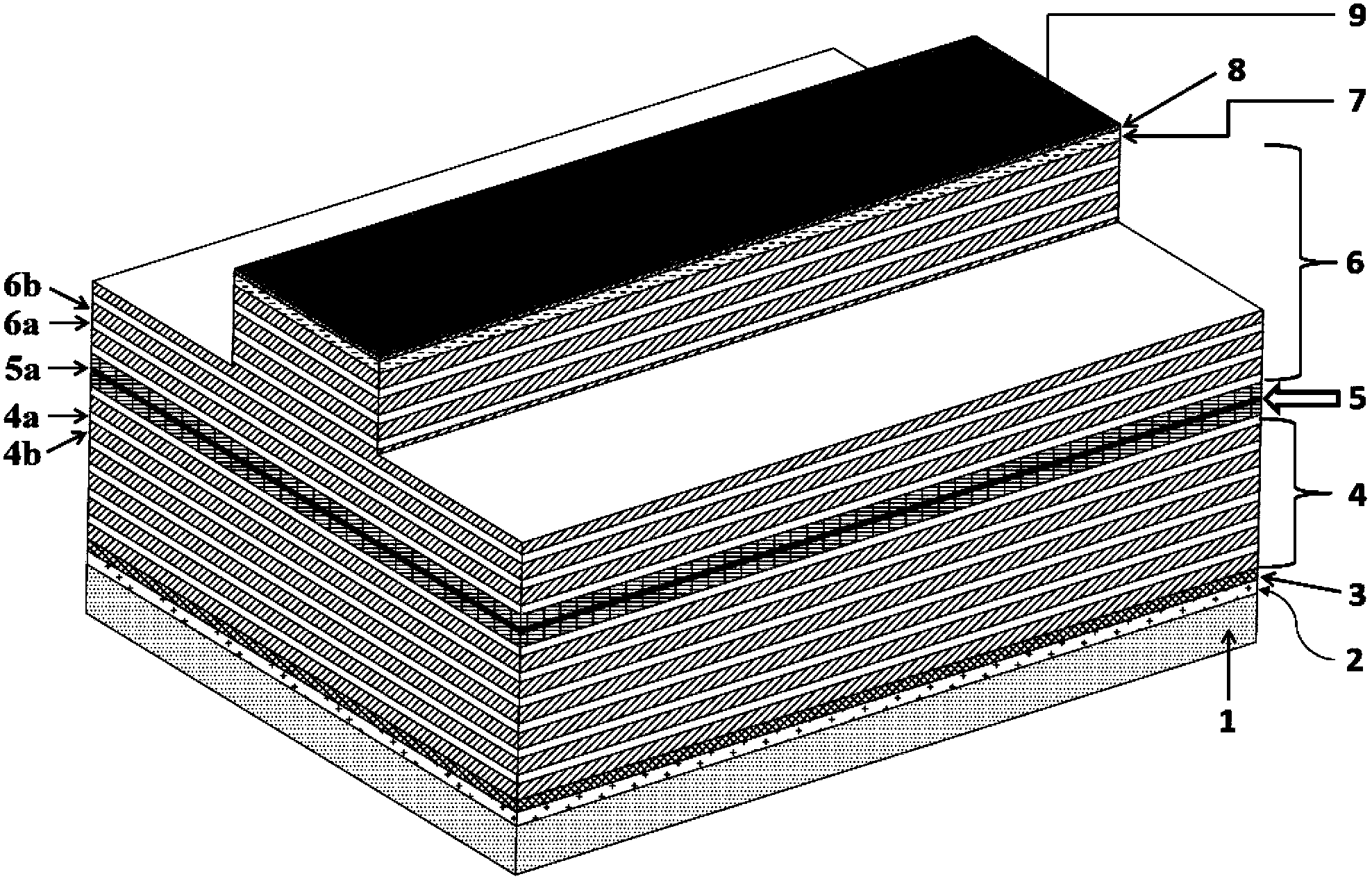
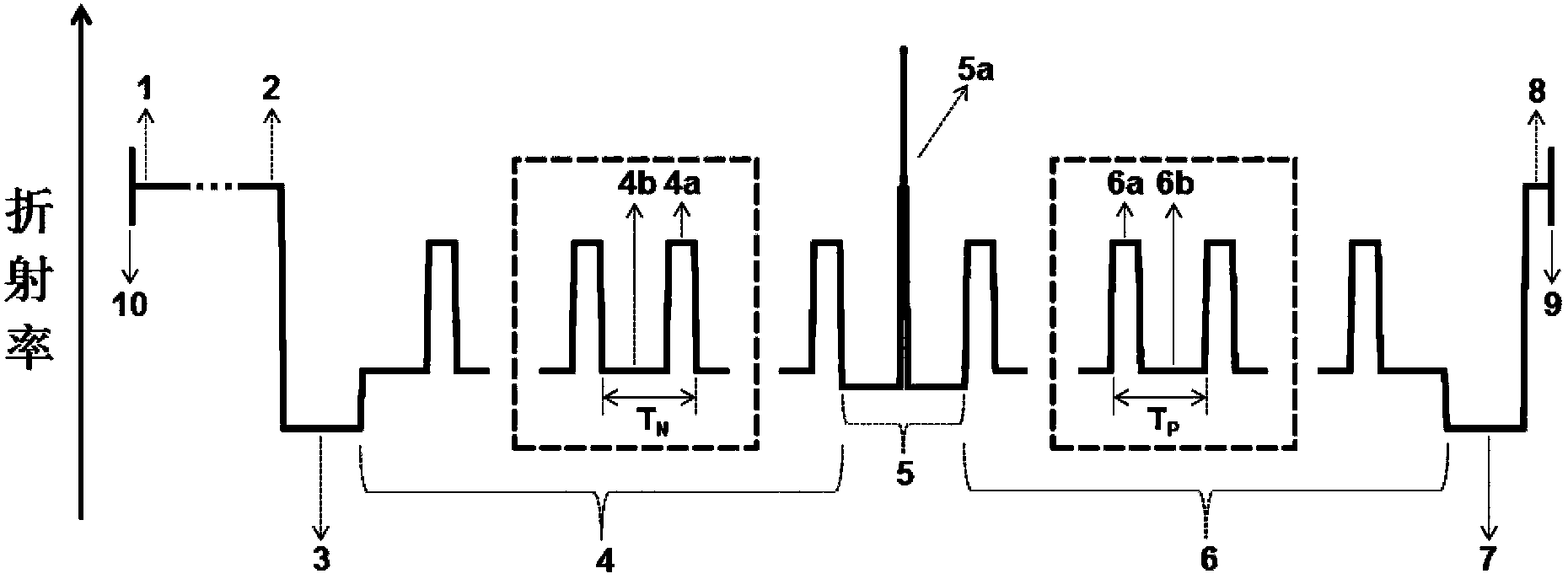
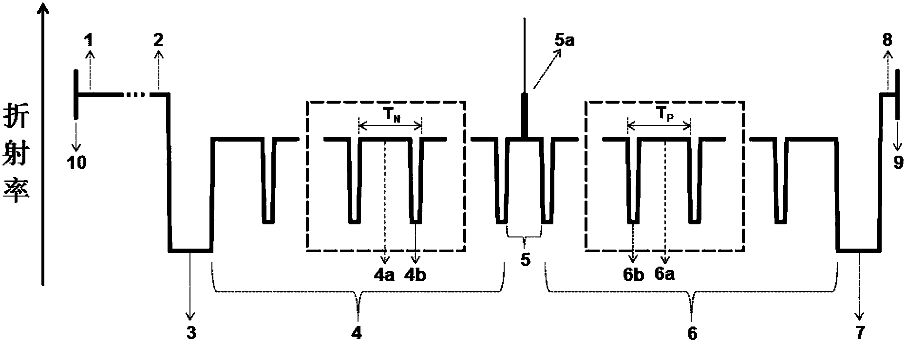
[0041] like Figure 4 (a), (b) and (c) are schematic diagrams of the refractive index distribution, near-field and far-field intensity distribution of the fundamental transverse mode of a 980nm wavelength Bragg reflective waveguide dual-beam laser. Its lower waveguide layer and upper waveguide layer are made of 6 pairs of Al with a thickness of 100nm / 600nm respectively. 0.1 Ga 0.9 As / Al 0.3 Ga 0.7 As periodic waveguide, where Al 0.1 Ga 0.9 As and Al 0.3 Ga 0.7 The refractive index of the As material is about 3.45 and 3.34 respectively; the material of the defect layer is Al 0.3 Ga 0.7 As, the thickness is 1300nm, the refractive index is 3.34; the active area uses In 0.2 Ga 0.8 As / GaAs quantum wells (QWs), located in the center of the defect layer. from Figure 4 (b) The near-field intensity distribution of the fundamental mode in (b) It can be seen that the near-field electric field distribution of the fundamental mode of the laser in the present invention is close...
Embodiment 2
[0043] like Figure 5 (a), (b) and (c) are schematic diagrams of the refractive index distribution, near-field and far-field intensity distribution of the fundamental transverse mode of a 980nm wavelength Bragg reflective waveguide dual-beam laser. Its lower waveguide layer and upper waveguide layer are made of 6 pairs of Al with a thickness of 100nm / 600nm respectively. 0.35 Ga 0.65 As / Al 0.1 Ga 0.9 As periodic waveguide, where Al 0.35 Ga 0.65 As and Al 0.1 Ga 0.9 The refractive index of the As material is 3.31 and 3.45 respectively; the material of the defect layer is Al 0.1 Ga 0.7 As, the thickness is 400nm, the refractive index is 3.45; the active area uses In 0.2 Ga 0.8 As / GaAs quantum wells (QWs). from Figure 4 (b) The near-field intensity distribution of the fundamental mode shows that even if the defect layer is made of a high-refractive material, by reducing its thickness, a near-field electric field distribution close to the cosine function can be obtaine...
Embodiment 3
[0045] like Image 6 (a), (b), and (c) are schematic diagrams of the refractive index distribution, near-field and far-field intensity distribution of the fundamental transverse mode of an 850nm wavelength Bragg reflective waveguide dual-beam laser. Its lower waveguide layer and upper waveguide layer are made of 8 pairs of Al with a thickness of 200nm / 500nm respectively. 0.15 Ga 0.85 As / Al 0.3 Ga 0.7 As periodic waveguide, where Al 0.15 Ga 0.85 As and Al 0.3 Ga 0.7 The refractive index of As material at 850nm wavelength is about 3.5 and 3.4 respectively; the defect layer material is 1μm thick Al 0.35 Ga 0.65 As, the refractive index is about 3.37. from Image 6 (b) It can be seen that when the lower confinement layer and the upper confinement layer do not exist, a stronger optical field confinement can still be obtained by increasing the period logarithm of the Bragg mirror, so that the leakage loss of the laser can be kept at a low level.
PUM
 Abstract
Description
Claims
Application Information


