Crystal wafer and diffusion method thereof
A technology of crystalline silicon wafer and diffusion method, which is applied in the field of solar cells, can solve problems such as difficulty in ensuring uniformity, high surface doping concentration, and increased process complexity, so as to increase open circuit voltage and short circuit current, reduce Auger recombination, Effects suitable for promotional applications
- Summary
- Abstract
- Description
- Claims
- Application Information
AI Technical Summary
Problems solved by technology
Method used
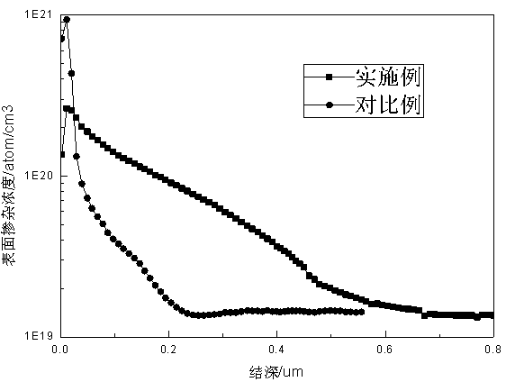
Image

Examples
Embodiment 1
[0035] 1. A diffusion method for a crystalline silicon wafer, comprising the steps of:
[0036] (1) Texture-making and cleaning the crystalline silicon wafer; the crystalline silicon wafer is a P-type polycrystalline silicon wafer with a resistivity of 1 to 3 Ω cm;
[0037] (2) Putting the above-mentioned crystalline silicon chip into a diffusion furnace for constant source diffusion, the atmosphere in the furnace is nitrogen, oxygen and pure nitrogen carrying phosphorus oxychloride, and the flow rate of the nitrogen carrying phosphorus oxychloride is 800 sccm, The flow rate of oxygen is 600 sccm, and the flow rate of pure nitrogen is 10 slm; the diffusion is variable temperature diffusion, the temperature is reduced from 840°C to 800°C, the diffusion time is 30min, and the sheet resistance after diffusion is 150 ohms / sq;
[0038] (3) Remove the phospho-silicate glass (PSG) from the silicon wafer after the above-mentioned constant source diffusion, and clean it;
[0039] (4) ...
PUM
 Abstract
Description
Claims
Application Information
 - R&D
- Intellectual Property
- Life Sciences
- Materials
- Tech Scout
- Unparalleled Data Quality
- Higher Quality Content
- 60% Fewer Hallucinations
Browse by: Latest US Patents, China's latest patents, Technical Efficacy Thesaurus, Application Domain, Technology Topic, Popular Technical Reports.
© 2025 PatSnap. All rights reserved.Legal|Privacy policy|Modern Slavery Act Transparency Statement|Sitemap|About US| Contact US: help@patsnap.com