Preparation method for three-dimensional carbon micro-nano electrode array structure integrating carbon nano-drape

A technology of electrode array and carbon nanometer, which is applied in the field of preparation of three-dimensional carbon micro-nano electrode array structure, to achieve the effect of enhancing stability and activation, enhancing electrical conductivity, and mature manufacturing process

Inactive Publication Date: 2012-10-31
HUAZHONG UNIV OF SCI & TECH
View PDF4 Cites 11 Cited by
  • Summary
  • Abstract
  • Description
  • Claims
  • Application Information

AI Technical Summary

Problems solved by technology

[0004] However, so far, the vast majority of studies on micro-nano film wrinkles are metal non-carbon structures, and mainly focus on the wrinkles on flat surfaces, and there is no report on the formation of film wrinkles by pyrolysis.

Method used


Image

  • Preparation method for three-dimensional carbon micro-nano electrode array structure integrating carbon nano-drape
  • Preparation method for three-dimensional carbon micro-nano electrode array structure integrating carbon nano-drape
  • Preparation method for three-dimensional carbon micro-nano electrode array structure integrating carbon nano-drape

Examples


Embodiment 1

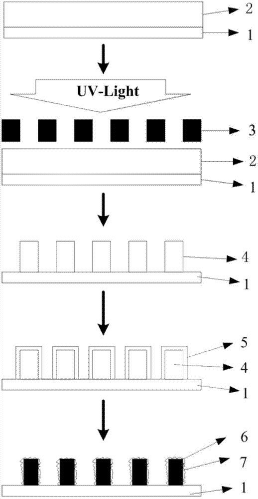
[0032] (1-1) Pretreatment steps: After rinsing with deionized water, place the silicon wafer in acetone for 10 minutes, then put it into SPM solution (concentrated sulfuric acid: hydrogen peroxide = 2:1), and heat it on a hot plate at 120°C for 10 minutes , after rinsing with deionized water, dry the substrate and cool to room temperature;

[0033] (1-2) Coating step: use the KW-4A type coagulation machine to homogenize the pretreated silicon substrate, and take two steps to apply the glue. The first step is to rotate at 500r / min for 50s, and then at a high speed of 1000r / min rotation 100s; pre-baking the obtained substrate after homogenization, heating on a hot plate at 65°C for 30min, and then heating at 120°C for 5min;

[0034] (1-3) Exposure step: Expose the pre-baked silicon substrate, the photolithography machine model is KarlSuss MA6, and the exposure dose is 5-7mW / cm 2 , the light wavelength is 365nm, and the exposure time is 100s; after the exposure, the substrate i...

Embodiment 2-7

[0052]

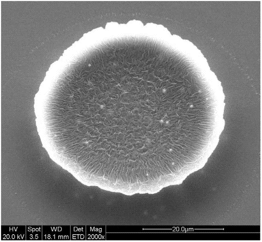
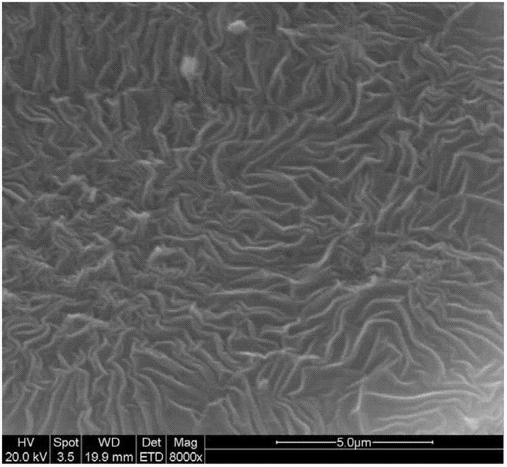
[0053] The results show that the thickness of the carbon film has an important influence on the formation of carbon wrinkles and the size of carbon wrinkles. The larger the thickness of the carbon film, the larger the size of the wrinkles. The maximum temperature has little effect on the formation of wrinkles, but since the minimum temperature required for complete carbonization of the photoresist needs to be achieved, the maximum temperature is required to be greater than 600°C. The heating rate from room temperature to 300 °C has little effect on the experiment, mainly because the photoresist does not react at this stage. The lower the heating rate from 300°C to 1000°C, the more conducive to the full shrinkage of carbon columns, which is also conducive to the formation of wrinkles. The carbonization process of the photoresist mainly occurs at this stage. At the same time, the photoresist (carbon column) shrinks. Since the Young's modulus of the deposited carbon ...


PUM

PropertyMeasurementUnit
thicknessaaaaaaaaaa
thicknessaaaaaaaaaa
thicknessaaaaaaaaaa

Abstract

The invention provides a preparation method for a three-dimensional carbon micro-nano electrode array structure integrating carbon nano-drape. The preparation method comprises the following steps: 1) photoetching to obtain a photoresist microstrucutre with an electrode pattern; 2) depositing a carbon film: depositing one layer of carbon film on the photoresist microstrucutre; and 3) performing pyrolysis: performing multi-step pyrolysis under the environment of inert gas or other mixed gas, wherein the pyrolysis temperature at each step is different. According to the preparation method, the carbon micro-nano integrated structure by combining the carbon nano-drape and the carbon microstructure and generating nano-drape on the surface of the microstructure. Due to integration of the biologically compatible nano-drape carbon film, the specific surface area of the carbon micro-nano electrode array is greatly increased and the bioactivity and the stability of the enzyme are improved. The method is applied to a micro-electro-mechanical system and has the characteristics of simple and convenient process, firm structure and high biocompatibility. The prepared carbon microstructure can serve as a microelectrode and can be applied to the micro-electro-mechanical fields of biological fuel cells, biological chips, micro-electrochemical sensors and the like.

Description

technical field [0001] The invention relates to a carbon micro / nano electromechanical system (C-MEMS / NEMS), in particular to a method for preparing a three-dimensional carbon micro-nano electrode array structure integrating carbon nano-folds. Background technique [0002] In recent years, with the continuous development of micro-electro-mechanical systems, carbon materials are expected to be applied in micro-electro-mechanical systems (MEMS) fields such as three-dimensional micro-batteries, biochips, micro-electrochemical sensors or molecular switches. One of the most promising is carbon microelectromechanical systems (C-MEMS) technology that combines conventional lithography with pyrolysis. Carbon MEMS technology is a manufacturing technology that combines thick photolithography technology with pyrolysis technology. This technology uses negative photoresist (mainly SU-8 glue) to form three-dimensional cross-linked microstructures after exposure, development and other steps....

Claims


Application Information

Patent Timeline
Patent Type & Authority Applications(China)
IPC IPC(8): B81C1/00
Inventor 汤自荣史铁林龙胡习爽刘丹徐亮亮廖广兰夏奇
Owner HUAZHONG UNIV OF SCI & TECH
Why Eureka
Try Eureka