RDL (radiological defense laboratory) technology-compatible inductive component and manufacture method

A technology of inductance components and inductances, applied in the direction of electrical components, semiconductor/solid-state device manufacturing, electric solid-state devices, etc., can solve problems such as unfavorable industrial production, polluting devices, complicated processes, etc. The effect of reducing packaging costs

Inactive Publication Date: 2012-11-14
SHANGHAI INST OF MICROSYSTEM & INFORMATION TECH CHINESE ACAD OF SCI
View PDF5 Cites 23 Cited by
  • Summary
  • Abstract
  • Description
  • Claims
  • Application Information

AI Technical Summary

Problems solved by technology

The disadvantage of the suspended inductor is that: on the one hand, the large void in the suspended inductor substrate needs to adopt MEMS technology, which is not compatible with the CMOS process, and it is difficult to realize the full chip integration of the RF receiver; on the other hand, the mechanical strength of the suspended inductor is small. Improving the mechanical strength of the suspension inductor often requires adding some cumbersome steps, which is not conducive to industrial production
However, the production of PN junction trenches increases the process steps and will pollute the existing devices on the wafer

Method used


Image

  • RDL (radiological defense laboratory) technology-compatible inductive component and manufacture method
  • RDL (radiological defense laboratory) technology-compatible inductive component and manufacture method
  • RDL (radiological defense laboratory) technology-compatible inductive component and manufacture method

Examples


Embodiment Construction

[0059] In order to fully demonstrate the advantages and positive effects of the present invention, the substantive features and remarkable progress of the present invention will be further described below in conjunction with the accompanying drawings and embodiments.

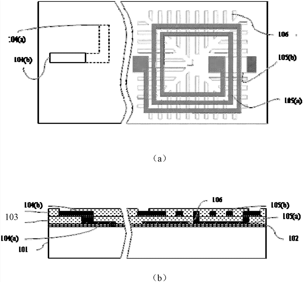
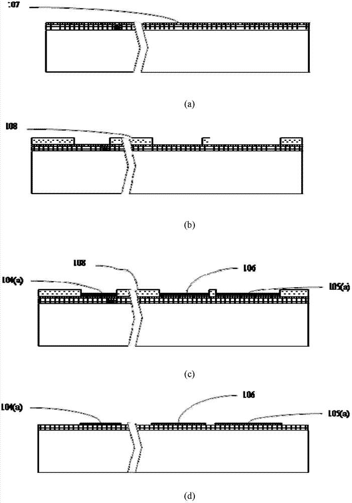
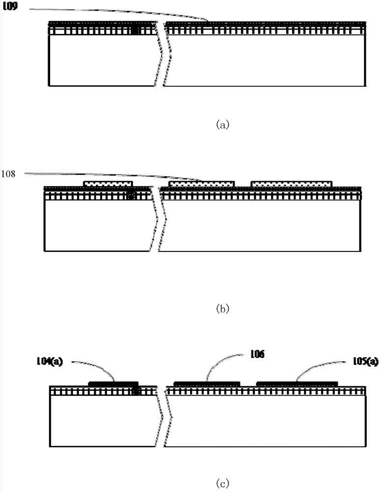
[0060] like figure 1 As shown, 106 is a ray-shaped metal shielding layer pattern, each of which has a width of 10 μm, and the shortest distance between two adjacent rays is 30 μm, and each ray is perpendicular to the corresponding side of the square spiral inductor directly above, effectively weakening the Eddy current. The first redistribution metal transmission layer 104 (a), the inductance bridge line 105 (a) and the radial metal shielding layer 106 are simultaneously deposited on the substrate 101 by a thin film process, and the substrate 101 can be a standard silicon chip or a chip embedded therein Ordinary silicon wafers. Passivation barrier layer 102 may be SiO 2 , a low dielectric constant medium or a...


PUM

PropertyMeasurementUnit
thicknessaaaaaaaaaa
thicknessaaaaaaaaaa
thicknessaaaaaaaaaa

Abstract

The invention relates to an RDL (radiological defense laboratory) technology-compatible inductive component and a manufacture method. The method is characterized by comprising the following steps of: using a thin film metal deposition technology on a silicon substrate and simultaneously forming a first layer metal interconnection transmission line and a shielding layer; carrying out the spin coating of a photosensitive medium layer, and developing in an exposure way, forming into a metal interconnection through hole, annealing, performing dry etching on plasmas to remove the developing remaining part, and filling the metal interconnection through hole with plated metal; forming a second layer metal interconnection transmission line and an inductance coil; forming an outermost layer metal through hole; and manufacturing an electrical inductor with the metal shielding layer under the condition that the original technological steps are not increased. The invention is compatible with the main-stream re-wiring technology in wafer level encapsulation, under the condition that the technological steps are not increased, the electrical inductor with the shielding layer can be manufactured at low cost, the substrate eddy current of the silicon substrate can be effectively cut off, the quality factor of the electric inductor can be improved, the series resistance of the electric inductor can be reduced, and the electromagnetic interference of the vortex current to a chip can be reduced.

Description

technical field [0001] The invention relates to an inductance element compatible with RDL technology and a manufacturing method, more specifically to a manufacturing of passive devices in wafer-level packaging, which can be used for inductance elements in redistribution layers (RDL) and a manufacturing method. Background technique [0002] With the development of wireless communication, radio frequency microwave circuits have been widely used in wireless personal communication, wireless local area network (WLAN), satellite communication, and automotive electronics. More and more functions are being continuously integrated into various handheld devices, while the size of the devices is also constantly shrinking. The demand for miniaturization, low cost, low power consumption, and high performance is continuously increasing. [0003] Inductors are heavily used in circuits and play an important role in matching networks, filters, low noise amplifiers. Traditional inductors re...

Claims


Application Information

Patent Timeline
Patent Type & Authority Applications(China)
IPC IPC(8): H01L23/522H01L23/552H01F27/36H01L21/02
Inventor 韩梅罗乐徐高卫王双福
Owner SHANGHAI INST OF MICROSYSTEM & INFORMATION TECH CHINESE ACAD OF SCI
Why Eureka
Try Eureka