Field effect transistor with diamond metal-insulator-semiconductor structure and preparation method thereof

A diamond and structure field technology, which is applied in semiconductor/solid-state device manufacturing, semiconductor devices, electrical components, etc., can solve problems such as low relative permittivity, affecting device transconductance characteristics, and material thickness can not be very thick, etc., to achieve Improve device gate control ability, reduce gate leakage, and weaken the effect of influence

Inactive Publication Date: 2013-01-30
NO 55 INST CHINA ELECTRONIC SCI & TECHNOLOGYGROUP CO LTD
View PDF3 Cites 16 Cited by
  • Summary
  • Abstract
  • Description
  • Claims
  • Application Information

AI Technical Summary

Problems solved by technology

However, the relative permittivity of these materials is not very high, therefore, the thickness of the materials used cannot be very thick
If the dielectric is too thick, it will affect the control ability of the gate to the channel, thus affecting the transconductance characteristics of the device

Method used


Image

  • Field effect transistor with diamond metal-insulator-semiconductor structure and preparation method thereof
  • Field effect transistor with diamond metal-insulator-semiconductor structure and preparation method thereof
  • Field effect transistor with diamond metal-insulator-semiconductor structure and preparation method thereof

Examples


Embodiment

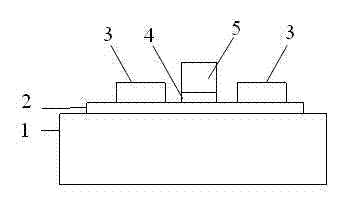
[0041] 1) First clean the surface of the single crystal diamond substrate material (5mm×5mm×0.5mm), ultrasonically clean it in acetone and ethanol solutions for 5 minutes, rinse it in deionized water, and blow it dry with nitrogen;

[0042] 2) Put the sample into the MPCVD equipment, the ionization source in the equipment is 2.45GHz, 1.2 kW, protected by pure hydrogen, and perform surface hydrogenation treatment at 500°C or 600°C or 700°C for 40 minutes;

[0043] 3) Use AZ7908 positive-type photoresist as a mask, and prepare the photoresist layer by spin coating method. The rotation speed of the coating is 5000rpm, and the coating time is 20 seconds. Curing the photoresist; using a photolithography machine to expose the required mask pattern, developing with RZX-3038 positive photoresist developer; after developing, harden the film in an oven at 90°C for 10 minutes; deposit metal Au in an electron beam evaporation table, The total thickness is 120nm; soak in acetone for 4 hour...


PUM

PropertyMeasurementUnit
thicknessaaaaaaaaaa

Abstract

The invention provides a field effect transistor with a diamond metal-insulator-semiconductor structure and prepared by means of an auto-oxidation method and a preparation method thereof. The field effect transistor with the diamond metal-insulator-semiconductor structure is structurally characterized in that a conducting channel is formed on a diamond after diamond surface is hydrogenated, two symmetrical Au are arranged on the conducting channel, a Al2O3 / TiO2 composite medium film is arranged between the two symmetrical Au, and a metal gate is arranged on the composite medium film. The preparation method comprises the steps of performing surface hydrogenation, performing ohmic contact, performing device isolation, preparing an Al2O3 / TiO2 multi-layer composite oxidization film, forming an insulating layer and forming a management information system (MIS) structure. The field effect transistor with the diamond metal-insulator-semiconductor structure has the advantages of effectively protecting the conducting channel layer on the surface of the diamond, adopting a TiO2 material with high dielectric constant to reduce the influence of the medium thickness on transconductance and frequency characteristics of a device, using a separating method to achieve an under-gate medium method, reducing the influence of a parasitic capacitor formed by a gate-side medium on the frequency performance of the device and obtaining a low-gate leakage range and a high-gate working voltage range.

Description

technical field [0001] The present invention relates to a diamond metal-insulator-semiconductor structure field-effect transistor prepared by an autoxidation method and a preparation method thereof, in which a multilayer composite thin-layer metal autoxidation film is combined on a diamond material with a conductive channel formed by surface hydrogenation The method realizes the preparation method of high-performance metal-insulator-semiconductor transistor device, and belongs to the technical field of semiconductor device preparation. technical background [0002] Diamond is composed of carbon element like graphite, but diamond is very different from graphite. Diamond is the hardest material in the world and is widely used in mechanical cutting, drilling and other fields. At the same time, diamond is also a very good semiconductor material, which has the characteristics of wide band gap, high thermal conductivity, high critical breakdown electric field, low dielectric cons...

Claims


Application Information

Patent Timeline
Patent Type & Authority Applications(China)
IPC IPC(8): H01L29/78H01L21/04
Inventor 周建军柏松孔岑陈堂胜
Owner NO 55 INST CHINA ELECTRONIC SCI & TECHNOLOGYGROUP CO LTD
Why Eureka
Try Eureka