Strain Si BiCMOS (Bipolar Complementary Metal Oxide Semiconductor) integrated device based on SOI SiGe HBT (Heterojunction Bipolar Transistor) and preparation method thereof

A technology for integrating devices and devices, which can be used in semiconductor/solid-state device manufacturing, electric solid-state devices, semiconductor devices, etc., and can solve problems such as limitations and low mobility of Si material carrier materials.

Inactive Publication Date: 2013-02-06
XIDIAN UNIV
View PDF3 Cites 2 Cited by
  • Summary
  • Abstract
  • Description
  • Claims
  • Application Information

AI Technical Summary

Problems solved by technology

[0007] Due to the low mobility of Si materials, the performance of integrated circuits manufactured by Si BiCMOS technology, especially the frequency performance, is greatly limited; for SiGe BiCMOS technology, although SiGe HBT is used for bipo...

Method used


Image

  • Strain Si BiCMOS (Bipolar Complementary Metal Oxide Semiconductor) integrated device based on SOI SiGe HBT (Heterojunction Bipolar Transistor) and preparation method thereof

Examples


Embodiment 1

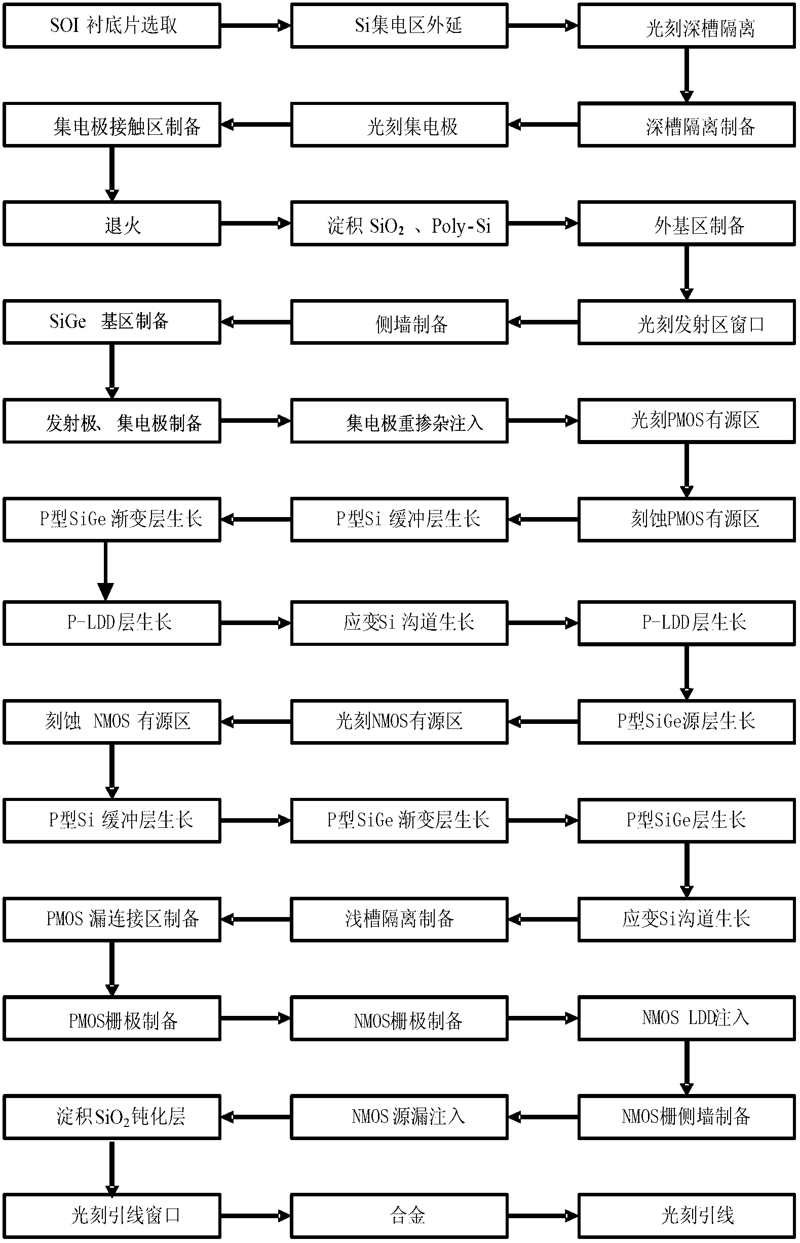
[0134] Embodiment 1: The strained Si BiCMOS integrated device and circuit based on SOI SiGe HBT with a channel length of 22nm are prepared, and the specific steps are as follows:

[0135] Step 1, epitaxial growth.

[0136] (1a) Select the SOI substrate, the support material of the lower layer of the substrate is Si, and the middle layer is SiO 2 , with a thickness of 150nm, and the upper material is doped with a concentration of 1×10 16 cm -3 N-type Si with a thickness of 100nm;

[0137] (1b) Using the chemical vapor deposition (CVD) method, at 600 ° C, grow a layer of N-type epitaxial Si layer with a thickness of 50 nm on the upper Si material, as the collector region, and the doping concentration of this layer is 1× 10 16 cm -3 .

[0138] Step 2, deep trench isolation preparation.

[0139] (2a) Using chemical vapor deposition (CVD), grow a layer of SiO with a thickness of 300 nm on the surface of the epitaxial Si layer at 600 °C. 2 layer;

[0140] (2b) Photoetched ...

Embodiment 2

[0209] Embodiment 2: The preparation of strained Si BiCMOS integrated device and circuit based on SOI SiGe HBT with a channel length of 30nm, the specific steps are as follows:

[0210] Step 1, epitaxial growth.

[0211] (1a) Select the SOI substrate, the support material of the lower layer of the substrate is Si, and the middle layer is SiO 2 , with a thickness of 300nm, and the upper material is doped with a concentration of 5×10 16 cm -3 N-type Si with a thickness of 120nm;

[0212] (1b) Using chemical vapor deposition (CVD), grow an N-type epitaxial Si layer with a thickness of 80nm on the upper Si material at 700°C as the collector region, and the doping concentration of this layer is 5× 10 16 cm -3 .

[0213] Step 2, deep trench isolation preparation.

[0214] (2a) Using chemical vapor deposition (CVD), grow a layer of SiO with a thickness of 400 nm on the surface of the epitaxial Si layer at 700 °C. 2 layer;

[0215] (2b) Photoetched deep trench isolation regi...

Embodiment 3

[0284] Embodiment 3: The strained Si BiCMOS integrated device and circuit based on SOI SiGe HBT with a channel length of 45nm are prepared, and the specific steps are as follows:

[0285] Step 1, epitaxial growth.

[0286] (1a) Select the SOI substrate, the support material of the lower layer of the substrate is Si, and the middle layer is SiO 2 , with a thickness of 400nm, and the upper material is doped with a concentration of 1×10 17 cm -3 N-type Si with a thickness of 150nm;

[0287] (1b) Using the method of chemical vapor deposition (CVD), grow a layer of N-type epitaxial Si layer with a thickness of 100nm on the upper layer of Si material at 750°C, as the collector region, and the doping concentration of this layer is 1× 10 17 cm -3 .

[0288] Step 2, deep trench isolation preparation.

[0289] (2a) Using chemical vapor deposition (CVD), grow a layer of SiO with a thickness of 500 nm on the surface of the epitaxial Si layer at 800 °C. 2 layer;

[0290] (2b) Pho...


PUM

PropertyMeasurementUnit
Thicknessaaaaaaaaaa
Thicknessaaaaaaaaaa
Thicknessaaaaaaaaaa

Abstract

The invention discloses a strain Si BiCMOS (Bipolar Complementary Metal Oxide Semiconductor) integrated device based on SOI SiGe HBT (Heterojunction Bipolar Transistor) and a preparation method thereof. The preparation method comprises the following steps: growing N-type Si epitaxy on a substrate, preparing a deep-trench isolator, forming a collector contact region, dryly etching to form a nitride side wall, wetly etching to form a base window, selectively growing a SiGe base region, and photoetching a collector window, removing Poly-Si to form a SiGe HBT device; photoetching an MOS (Metal Oxide Semiconductor) device active area groove, respectively and continuously growing Si buffer layer, gradient SiGe layer, fixed component SiGe layer, N-type strain Si channel layer, Si buffer layer and the like in the MOS device active area groove, and preparing a drain electrode and a grid electrode to form a PMOS (Positive channel Metal Oxide Semiconductor) device; and preparing an NMOS (Negative channel Metal Oxide Semiconductor) device grid dielectric layer and a grid polycrystal to form an NMOS device. The characteristic of tension strain Si material such as mobility anisotropy is fully utilized to prepare the BiCMOS integrated device with strengthened performance and a circuit thereof.

Description

technical field [0001] The invention belongs to the technical field of semiconductor integrated circuits, and in particular relates to a strained Si BiCMOS integrated device based on SOI SiGe HBT and a preparation method. Background technique [0002] The integrated circuit, which appeared in 1958, is one of the most influential inventions of the 20th century. Microelectronics based on this invention has become the basis of existing modern technology, accelerating the process of knowledge and informationization of human society, and at the same time changing the way of thinking of human beings; it not only provides human beings with powerful It is not only a tool for transforming nature, but also opens up a broad space for development. [0003] Semiconductor integrated circuits have become the basis of the electronics industry. People's huge demand for the electronics industry has prompted the rapid development of this field; in the past few decades, the rapid development o...

Claims


Application Information

Patent Timeline
IPC IPC(8): H01L27/12H01L21/84
Inventor 张鹤鸣王海栋胡辉勇宋建军宣荣喜舒斌戴显英郝跃
Owner XIDIAN UNIV
Why Eureka
Try Eureka