Preparation method of polyaniline and II-VI family semiconductor compound photovoltaic conversion film

A II-VI, photoelectric conversion technology, applied in the direction of semiconductor devices, circuits, electrical components, etc., can solve the problems of difficult processing, easy agglomeration of semiconductor nanoparticles, and can not be directly used for application, and achieves inhibition of agglomeration, sulfide or selenium. Simple process and strong operability

Inactive Publication Date: 2014-12-24
BEIJING UNIV OF CHEM TECH
View PDF3 Cites 0 Cited by
  • Summary
  • Abstract
  • Description
  • Claims
  • Application Information

AI Technical Summary

Problems solved by technology

However, semiconductor nanoparticles are easy to agglomerate and difficult to process and form, so that they are often not directly used in practice, but are usually compounded into other substrates in a certain form.

Method used


Image

  • Preparation method of polyaniline and II-VI family semiconductor compound photovoltaic conversion film
  • Preparation method of polyaniline and II-VI family semiconductor compound photovoltaic conversion film
  • Preparation method of polyaniline and II-VI family semiconductor compound photovoltaic conversion film

Examples


Embodiment 1

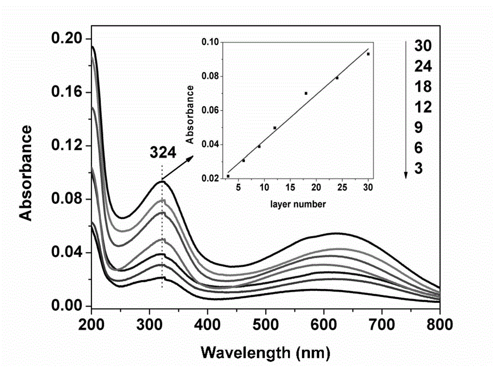
[0022] (1) Prepare a mixed solution of zinc nitrate, aluminum nitrate and urea, in which Zn 2+ At a concentration of 10mM, Al 3+ The concentration is 5mM, the urea concentration is 35mM, the above mixed solution is magnetically stirred and refluxed at 97°C for two days, then centrifuged and dried, and the obtained product is ZnAl-CO 3 LDH;

[0023] Take 1g ZnAl-CO 3 Disperse LDH in 90mL of methanol, then add 6.64mmol of nitric acid, stir for 3-5h, and pass nitrogen protection during this process; after the reaction, filter, rinse with methanol, and dry to obtain ZnAl-NO 3 LDH;

[0024] (2) Weigh 0.5g ZnAl-NO 3 LDH was added to 500mL formamide solution, magnetically stirred for 72h, centrifuged, and the precipitate was discarded to obtain a clear and transparent colloidal solution A;

[0025] (3) First, pretreat the quartz wafer, silicon wafer and ITO conductive glass: soak the quartz wafer or silicon wafer in a mixture of methanol and 37wt% hydrochloric acid for 20 minute...

Embodiment 2

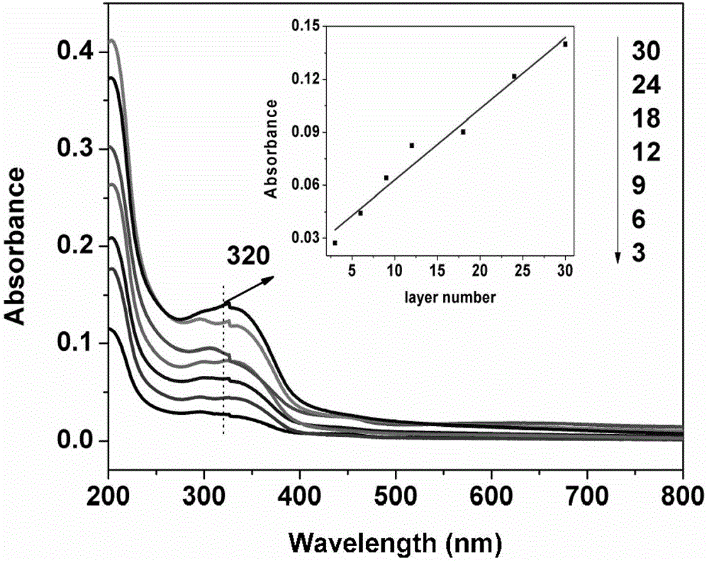
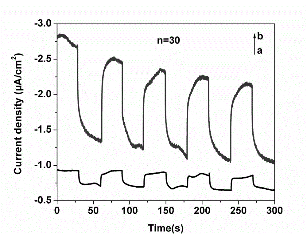
[0032] In-situ selenization of the polyaniline and hydrotalcite multilayer composite film prepared in Example 1: immerse the prepared polyaniline and hydrotalcite multilayer composite film in freshly prepared NaHSe solution, the concentration of NaHSe solution is 0.2M, The reaction time is 1 h, and the nitrogen is protected during the selenization process.

Embodiment 3

[0034] (1) Prepare a mixed solution of zinc nitrate, cadmium nitrate, aluminum nitrate and urea, in which Zn 2+ At a concentration of 8mM, Cd 2+ At a concentration of 2mM, Al 3+ The concentration is 5mM, the urea concentration is 35mM, the above mixed solution is magnetically stirred and refluxed at 97°C for two days, then centrifuged and dried, and the obtained product is ZnCdAl-CO 3 LDH;

[0035] Take 1gZnCdAl-CO 3 Disperse LDH in 90mL of methanol, then add 6.64mmol of nitric acid, stir for 3-5h, and pass nitrogen protection during this process; after the reaction, filter, rinse with methanol, and dry to obtain ZnCdAl-NO 3 LDH;

[0036] (2) ZnCdAl-NO 3 LDH stripping method is the same as embodiment 1;

[0037] (3) Same as embodiment 1;

[0038] (4) Same as embodiment 1.


PUM


Abstract

The invention discloses a polyaniline and II-VI family semiconductor nano particle compound photovoltaic conversion film with photoelectric conversion property, and a preparation method thereof. The preparation method comprises the steps of: firstly, self-assembling polyaniline and a stripped hydrotalcite nano sheet into a film by adopting a layer by layer self-assembly technology; and then carrying out in situ vulcanization or selenylation to prepare the polyaniline and II-VI family semiconductor compound photovoltaic conversion film. Through subject or object body ordered assembly, polyaniline is uniformly dispersed among hydrotalcite layers, and plays a role in stabilizing the polyaniline structurally and a role in promoting properties of light, electricity, catalysis and the like on the polyaniline from the function; and according to the polyaniline and II-VI family semiconductor compound photovoltaic conversion film obtained through fixed point vulcanization or selenylation, the polyaniline and the hydrotalcite are used as dual matrixes of an II-VI family semiconductor structurally, thus agglomeration of the II-VI family semiconductor can be effectively inhibited, heterogeneous junctions formed by the polyaniline and the II-VI family semiconductor from the performance, and photoelectric properties can be improved.

Description

technical field [0001] The invention belongs to the field of polymer and semiconductor nanoparticle composite film preparation, in particular to a composite photoelectric conversion film of polyaniline and II-VI semiconductor nanoparticle with photoelectric conversion performance and a preparation method thereof. Background technique [0002] II-VI semiconductor nanoparticles (quantum dots) have unique quantum size effects and surface effects because their radii are smaller than or close to the exciton Bohr radius, and exhibit optical, electrical and photoelectric conversion characteristics different from those of bulk semiconductors. It has great R&D attractiveness and application prospects in the fields of high-efficiency solar cells, quantum dot lasers, bio-labels, and light-emitting diodes. However, semiconductor nanoparticles are easy to agglomerate and difficult to process and form, which makes them often not directly used in practice, but usually compounded into other...

Claims


Application Information

Patent Timeline
Patent Type & Authority Patents(China)
IPC IPC(8): H01L31/0256
Inventor 郭影徐冬梅关美玉
Owner BEIJING UNIV OF CHEM TECH
Why Eureka
Try Eureka