Low-cost low-pollution gallium nitride nano-wire preparation generation method

A gallium nitride nanowire and low-pollution technology, applied in nanotechnology, nanotechnology, nanotechnology, etc. for materials and surface science, can solve complex and expensive system equipment, unfavorable large-scale production, reactants or by-products Harmful to the human body or the environment, etc., to achieve the effect of simple equipment and excellent field emission performance

Active Publication Date: 2013-02-20
BEIJING UNIV OF TECH
View PDF4 Cites 10 Cited by
  • Summary
  • Abstract
  • Description
  • Claims
  • Application Information

AI Technical Summary

Problems solved by technology

At present, curved or straight gallium nitride nanowires have been obtained by chemical vapor deposition, pulsed laser deposition, metal-organic chemical vapor deposition, molecular beam epitaxy, etc., but these methods have serious defects. , such as complex and expensive system equipment, reactants or by-products are harmful to the human body or the environment, or are not conducive to the realization of large-scale production

Method used


Image

  • Low-cost low-pollution gallium nitride nano-wire preparation generation method
  • Low-cost low-pollution gallium nitride nano-wire preparation generation method
  • Low-cost low-pollution gallium nitride nano-wire preparation generation method

Examples


Embodiment 1

[0021] (1) The GaN powder is mixed with glue, ground, passed through an 80-mesh sieve, pressed into tablets, calcined at 560°C for 2 hours, and fired into a powder target. The preparation of powder targets in the prior art is a mature technology, and a slight change in the above parameters is also necessary for

[0022] Product performance is basically unaffected.

[0023] (2) Deposit the cleaned and dried silicon wafer in a SBC-12 small ion sputtering apparatus for 30s to obtain a substrate with a gold film with a thickness of about 10nm on the surface.

[0024] (3) The GaN powder target and substrate prepared by the above method, using the plasma-assisted hot wire chemical vapor deposition method: at a pressure of 1500Pa, a substrate temperature of 900°C, a bias current of 120mA, and a nitrogen flow rate of 40cm 3 / min, the hydrogen flow rate is 10 cm 3 / min, the deposition time is 5min, and GaN nanometers are obtained.

Embodiment 2

[0026] (1) The GaN powder is mixed with glue, ground, passed through an 80-mesh sieve, pressed into tablets, calcined at 560°C for 2 hours, and fired into a powder target.

[0027] (2) Deposit the cleaned and dried silicon wafer in a SBC-12 small ion sputtering apparatus for 30s to obtain a substrate with a gold film with a thickness of about 10nm on the surface.

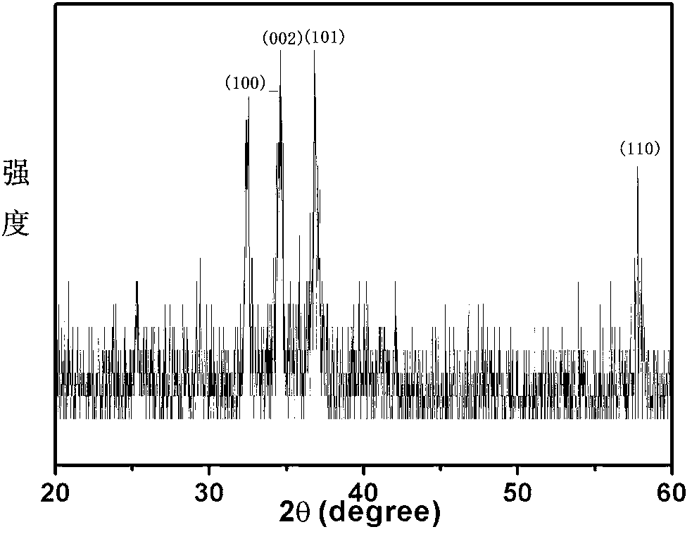
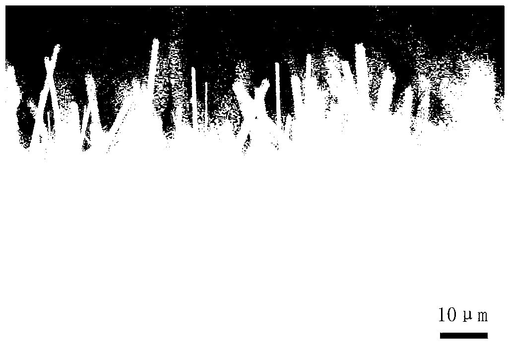
[0028] (3) The GaN powder target and substrate prepared by the above method, using the plasma-assisted hot wire chemical vapor deposition method: at a pressure of 1500Pa, a substrate temperature of 900°C, a bias current of 120mA, and a nitrogen flow rate of 40cm 3 / min, the hydrogen flow rate is 10 cm 3 / min, the deposition time is 20min, and GaN nanowires are obtained, and its XRD pattern is shown in figure 1 , and its SEM spectrum is shown in figure 2 , see its Raman spectrum Figure 4 , and its field emission current density spectrum is shown in Figure 6 .

Embodiment 3

[0030] (1) The GaN powder is mixed with glue, ground, passed through an 80-mesh sieve, pressed into tablets, calcined at 560°C for 2 hours, and fired into a powder target.

[0031] (2) Deposit the cleaned and dried silicon wafer in a SBC-12 small ion sputtering apparatus for 30s to obtain a substrate with a gold film with a thickness of about 10nm on the surface.

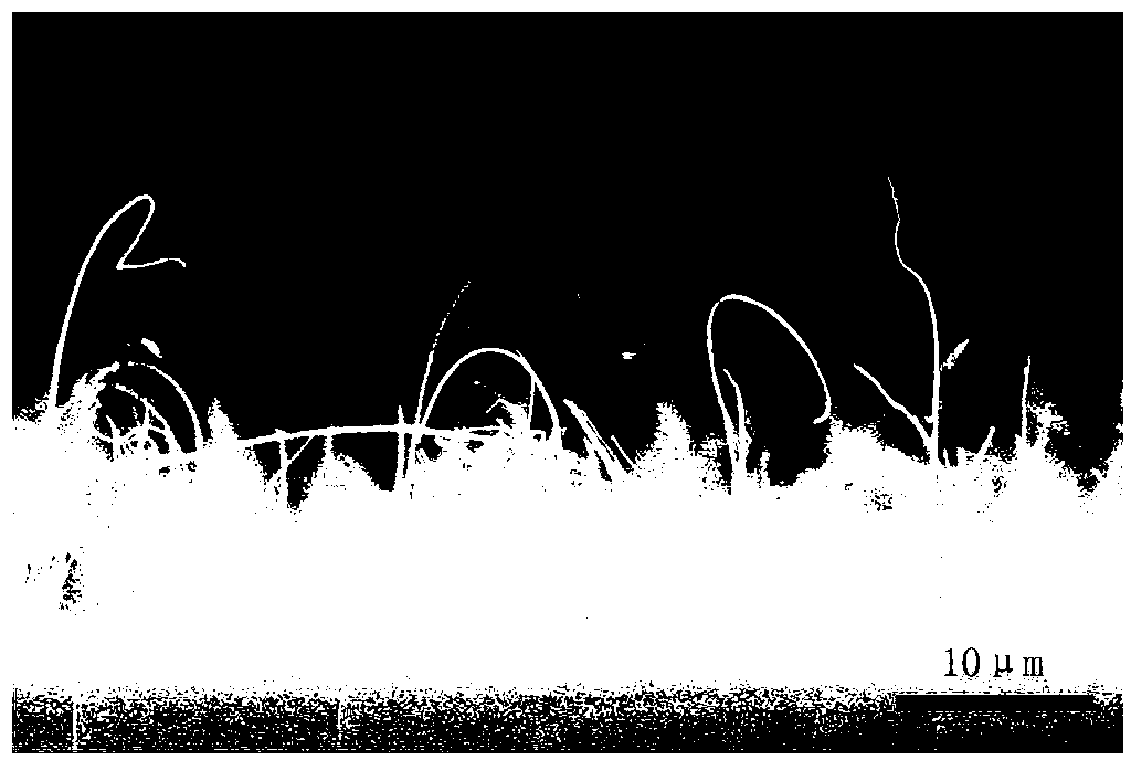
[0032] (3) The GaN powder target and substrate prepared by the above method, using the plasma-assisted hot wire chemical vapor deposition method: at a pressure of 1500Pa, a substrate temperature of 900°C, a bias current of 120mA, and a nitrogen flow rate of 40 cm 3 / min, the hydrogen flow rate is 10 cm 3 / min, the deposition time is 30min, and GaN nanowires are obtained, and its SEM diagram is shown in image 3 .


PUM

PropertyMeasurementUnit
diameteraaaaaaaaaa
lengthaaaaaaaaaa

Abstract

The invention relates to a low-cost low-pollution gallium nitride (GaN) nano-wire preparation generation method, and belongs to the field of inorganic compound semiconductor materials. The method provided by the invention comprises the steps that: (1) GaN powder is subjected to gum-doping, grinding, tabletting, and calcining, such that a GaN target is prepared; (2) a washed and bake-dried silicon wafer is deposited for 30-60s by using a SBC-12 small ion sputtering instrument, such that a substrate with a gold film with a thickness of 10-30nm on the surface is obtained; and (3) a plasma-assisted hot-wire chemical vapor deposition method is utilized, wherein an atmospheric pressure is 1500Pa-2500Pa, a substrate temperature is 800-1000 DEG C, a bias current is 100mA-180mA, a flow rate of fed nitrogen is 10-50cm<3>/min, a flow rate of fed hydrogen is 10-50cm<3>/min, and a deposition time is 5-30min. With the method provided by the invention, solid and linear gallium nitride nano-wires can be obtained. The product is straight, neat, ordered, uniform, and linear. Chemical and physical properties of the nano-wires are stable. The preparation process is short, and product growth is fast. Product diameter reaches 40-150nm, and an average single wire length is 10-15mum.

Description

technical field [0001] The invention relates to a low-cost and low-pollution method for preparing gallium nitride nanowires, and belongs to the technical field of preparation and generation methods of inorganic compound semiconductor materials. Background technique [0002] GaN-based semiconductor materials are new semiconductor materials for the development of optoelectronic devices and microelectronic devices, and together with semiconductor materials such as silicon carbide (SiC) and diamond, are known as the first generation of Ge, Si semiconductor materials, the second generation of GaAs, InP The third generation of semiconductor materials after compound semiconductor materials. GaN has a wide direct band gap (band gap Eg>2.3eV), which can be used to make blue light-emitting diodes (LEDs) and blue-violet laser diodes (LDs), and has good development in full-color display, semiconductor lighting, data storage, etc. Prospect. GaN material belongs to the direct transit...

Claims


Application Information

Patent Timeline
Patent Type & Authority Applications(China)
IPC IPC(8): C01B21/06B82Y30/00C23C16/34C23C16/52
Inventor 王如志王宇清严辉朱满康侯育冬王波张铭宋雪梅刘晶冰汪浩
Owner BEIJING UNIV OF TECH
Why Eureka
Try Eureka