Conductive layer transfer material and touch panel

A technology for transfer printing materials and conductive layers, applied to conductive materials, conductive materials, conductive layers on insulating carriers, etc., can solve problems such as inability to conform to conductive layers, use restrictions, and insulation of glass substrates, etc., to improve uniformity of transfer printing Good adhesion and unevenness, fewer parts

Inactive Publication Date: 2013-03-13
FUJIFILM CORP
View PDF39 Cites 23 Cited by
  • Summary
  • Abstract
  • Description
  • Claims
  • Application Information

AI Technical Summary

Problems solved by technology

However, in this proposal, the conductive layer and the photosensitive resin layer are different layers, so the conductive layer does not make electrical contact with the electrodes on the glass substrate, and there are limitations in use.
[0005] On the other hand, when the conductive layer also serves as the photosensitive resin layer, although it is electrically contacted with the electrodes on the glass substrate, there is a problem that if the conductive layer is thin, the electrodes on the glass substrate will and other unevenness, the conductive layer across the unevenness cannot conform to the unevenness on the glass substrate and has insulation problems

Method used


Image

  • Conductive layer transfer material and touch panel
  • Conductive layer transfer material and touch panel
  • Conductive layer transfer material and touch panel

Examples


example

[0286] Hereinafter, examples of the present invention will be described, but the present invention is not limited by these examples.

[0287] In the following examples, the average thickness of the substrate, the average thickness of the conductive layer, and the average thickness of the buffer layer were measured as follows.

[0288]

[0289] It can be measured by the following method: SEM observation is performed after exposing the cross-section of the material by cutting with a microtome, or TEM observation is performed on a slice made by a microtome after embedding with epoxy resin. The average thickness of these base materials and each layer is the average value measured at 10 places.

Synthetic example 1

[0291]

[0292]Using 7.79g (grams) of methacrylic acid (MAA) and 37.21g of benzyl methacrylate (BzMA) as the monomer components constituting the copolymer, and 0.5g of azobisisobutyronitrile (AIBN) as the radical polymerization initiator Agent, these compounds are polymerized in 55.00 g of solvent propylene glycol monomethyl ether acetate (PGMEA), thereby obtaining the PGMEA solution (solid content concentration) of the binder (A-1) represented by the following formula: 45% by mass). In addition, the polymerization temperature is adjusted to a temperature of 60°C to 100°C.

[0293] The weight average molecular weight (Mw) of the binder (A-1) was measured using gel permeation chromatography (GPC). As a result, the weight average molecular weight (Mw) in terms of polystyrene was 30,000, and the molecular weight distribution (Mw / Mn) was 2.21.

[0294] [Chem 3]

[0295]

[0296] (modulation example 1)

[0297] -Preparation of silver nanowire aqueous dispersion-

[0298]...

example 1

[0321]

[0322] "The Formation of the Buffer Layer"

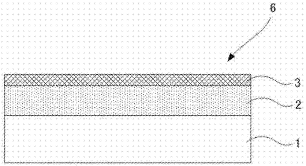
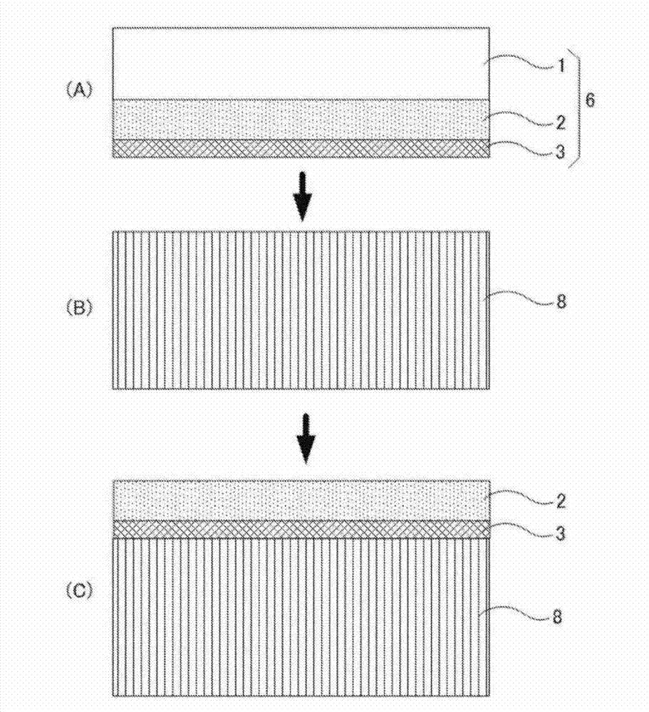
[0323] On a polyethylene terephthalate (PET) film having an average thickness of 30 μm as a substrate, a buffer layer coating solution having the following composition was applied and dried to form a buffer layer with an average thickness of 10 μm.

[0324] -Composition of coating liquid for buffer layer-

[0325] Methyl methacrylate / 2-ethylhexyl acrylate / benzyl methacrylate / methacrylic acid copolymer (copolymerization composition ratio (molar ratio)=55 / 30 / 10 / 5, weight average molecular weight=100,000 , glass transition temperature (Tg) = 70°C) 6.0 parts by mass

[0326] ・Styrene / acrylic acid copolymer (copolymer composition ratio (molar ratio) = 65 / 35, weight average molecular weight = 10,000, glass transition temperature (Tg) = 100° C.) 14.0 parts by mass

[0327] · BPE-500 (manufactured by Shin-Nakamura Chemical Co., Ltd.) · · · 9.0 parts by mass

[0328] · Megafac F-780-F (manufactured by Dainippon Ink Chemical Ind...


PUM

PropertyMeasurementUnit
lengthaaaaaaaaaa
thicknessaaaaaaaaaa
thicknessaaaaaaaaaa

Abstract

Disclosed are: a conductive layer transfer material which has good transferability and adhesion to a transfer-receiving body and exhibits improved transfer uniformity of a conductive layer; and a touch panel, which has a conductive layer that is transferred using the conductive layer transfer material, and which is reduced in the number of components and can be formed lightweight and thin. Specifically disclosed is a conductive layer transfer material which comprises: a base; and a cushion layer and a conductive layer that are arranged on the base in this order, said conductive layer containing metal nanowires that have an average minor axis length of 100 nm or less and an average major axis length of 2 [mu]m or more. The total average thickness (A) of the conductive layer and the cushion layer and the average thickness (B) of the base satisfy the relation: A / B = 0.1-0.7. The conductive layer has an average thickness of 0.01-0.2 [mu]m, and the cushion layer has an average thickness of 1-50 [mu]m.

Description

technical field [0001] The invention relates to a conductive layer transfer material and a touch panel. Background technique [0002] In recent years, touch panels are mounted on display devices such as liquid crystal panels and electronic paper as input devices. However, in the case of a capacitive touch panel, two or more pieces of transparent glass with indium tin oxide (ITO) are used, so the yield (yield) at the time of bonding is deteriorated, and there is a reduction There is an urgent need to reduce the thickness of the touch panel while reducing the number of parts. Furthermore, there is an urgent need for cost reduction by reducing the number of materials used. Therefore, an on-cell (on-cell) system in which an ITO transparent conductive material is laminated on the surface of a liquid crystal cell has been disclosed (see Non-Patent Document 1). However, this Non-Patent Document 1 only discloses a configuration using ITO as a transparent conductive film, which in...

Claims


Application Information

Patent Timeline
Patent Type & Authority Applications(China)
IPC IPC(8): H01B13/00B32B27/18G06F3/041H01B5/14
CPCH01B1/00G06F3/044B32B27/20G06F3/045B32B2457/202G06F3/0443G06F3/0446Y10T428/24975
Inventor 冈崎贤太郎松并由木小畑史生直井宪次中平真一
Owner FUJIFILM CORP
Why Eureka
Try Eureka