

Light-emitting diode and preparation method thereof
A technology of light-emitting diodes and light-emitting layers, which is applied in the fields of semiconductor/solid-state device manufacturing, semiconductor devices, electrical components, etc., can solve the problems of poor charge transfer capability of quantum dots and affect the luminous efficiency of light-emitting diodes, and achieve high luminous efficiency and high-efficiency optoelectronics. The effect of conversion, efficient transfer of charge
- Summary
- Abstract
- Description
- Claims
- Application Information
AI Technical Summary
Problems solved by technology
Method used
Image

Examples
Embodiment 1
[0033] Embodiment 1: the preparation of graphene / CdS quantum dot composite material.
[0034] Take a graphite oxide solution with a concentration of 0.5 mg / ml, add a certain amount of cadmium acetate dihydrate and mix, and the amount of the two is calculated by molar mass ratio, that is, graphite oxide: cadmium acetate dihydrate = 1:1; the mixture is evenly dispersed in In a certain volume of dimethyl sulfoxide solution, the amount of dimethyl sulfoxide solution is calculated based on the quality of graphite oxide, that is, 1 milliliter of dimethyl sulfoxide solution needs to be added for every 1 mg of graphite oxide; , transferred to a high-temperature reactor, and annealed at 180° C. for 12 hours. The product was repeatedly washed with acetone and ethanol, and then dried to obtain a graphene / CdS quantum dot composite material.
[0035] Of course, to realize the present invention, any graphene / quantum dot composite material preparation method disclosed in the prior art can al...
Embodiment 2
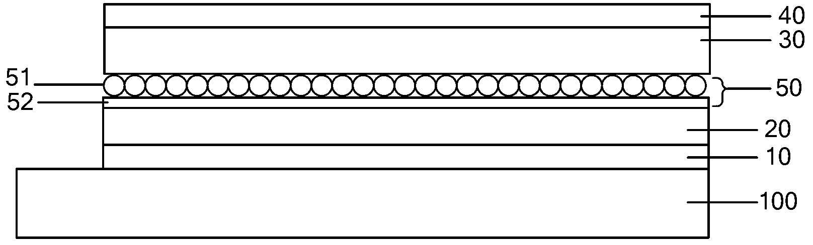
[0037] The method for preparing a light-emitting diode comprising a graphene / quantum dot light-emitting layer in this embodiment is:
[0038] 1) Deposit a layer of metal cathode 10 on the substrate 100 by sputtering, vapor deposition, spin coating and other methods;
[0039] 2) Depositing an electron transport layer 20 by sputtering, evaporation, spin coating and other methods;
[0040] 3) Dissolving the graphene / quantum dot composite material in an organic solvent such as toluene, coating it on the surface of the electron transport layer 20 by spin coating, etc., heating to remove the solvent, and forming an empty graphene / quantum dot light emitting layer 50;
[0041] 4) Deposit a layer of hole transport layer 30 by sputtering, vapor deposition, spin coating and other methods using triphenyldiamine as the material of the hole transport layer;
[0042] 5) Deposit a layer of transparent anode 40 by sputtering, vapor deposition, spin coating and other methods.
[0043] The qua...
Embodiment 3
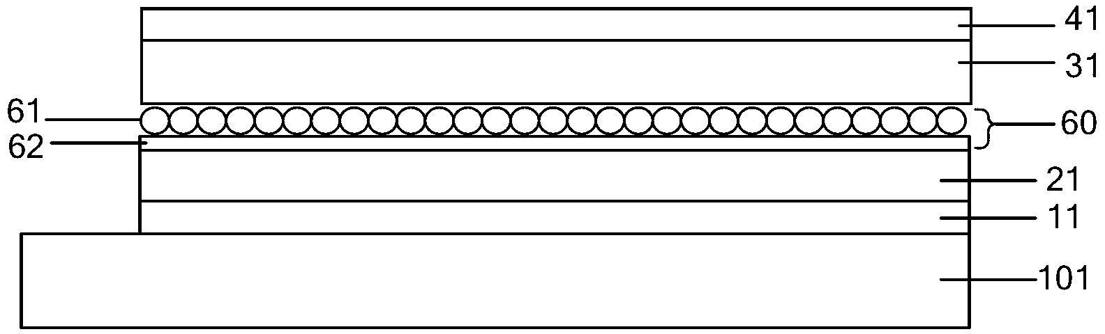
[0052] The method for preparing a light-emitting diode comprising a graphene / quantum dot light-emitting layer in this embodiment is:
[0053] 1) Deposit a layer of transparent anode 11 on the substrate 101 by sputtering, evaporation, spin coating and other methods;
[0054] 2) Dissolving the graphene / quantum dot composite material and the hole transport layer material triphenyldiamine in an organic solvent such as toluene, and coating it on the surface of the transparent anode 11 by spin coating or other methods;
[0055] 3) removing the solvent by heating to form the hole transport layer 21 and the graphene / quantum dot light-emitting layer 60 covering the hole transport layer 21;
[0056] 4) Depositing an electron transport layer 31 by sputtering, evaporation, spin coating and other methods;
[0057] 5) Deposit a layer of metal cathode 41 by sputtering, vapor deposition, spin coating and other methods.
[0058] In the preparation of the hole transport layer (electron transp...
PUM
 Abstract
Description
Claims
Application Information