Method for preparing three-dimensional hollow micro nanometer functional structure by utilizing laser direct writing

A micro-nano structure, three-dimensional hollow technology, applied in the manufacture of microstructure devices, microstructure technology, microstructure devices, etc., can solve the problems of complex preparation methods, inability to freely design, inefficiency, etc., to reduce the difficulty of the process and increase the function. , to achieve the effect of functional optimization

Active Publication Date: 2013-04-03
INST OF PHYSICS - CHINESE ACAD OF SCI
View PDF6 Cites 26 Cited by
  • Summary
  • Abstract
  • Description
  • Claims
  • Application Information

AI Technical Summary

Problems solved by technology

[0004] The purpose of the present invention is to provide a method for preparing three-dimensional hollow micro-nano functional structures by laser direct writing, using a method based on two-photon polymerization to prepare photoresists with various heights, side lengths and cross-sectional geometries on hollow substrates The polymer hollow three-dimensional micro-nano structure, through the growth of functional materials, realizes the function

Method used


Image

  • Method for preparing three-dimensional hollow micro nanometer functional structure by utilizing laser direct writing
  • Method for preparing three-dimensional hollow micro nanometer functional structure by utilizing laser direct writing

Examples


Embodiment 1

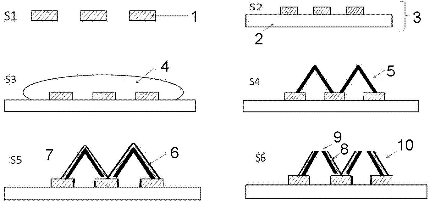
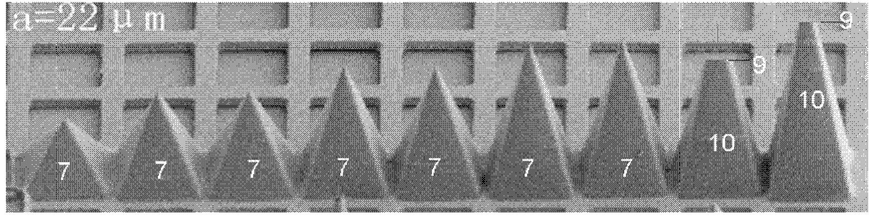
[0044] Embodiment 1: Utilize the preparation method of the present invention, adopt three-dimensional laser direct writing technology to directly prepare the pyramid structure of arbitrary height and side length, and realize the functionalization of photoresist polymer three-dimensional hollow micro-nano structure by electron beam deposition method, specifically Proceed as follows:

[0045] (1) The TEM copper grid 1 with a square grid and the quartz glass 2 were ultrasonically cleaned with acetone, ethanol, and deionized water in sequence, rinsed with isopropanol, and then dried with nitrogen.

[0046] (2) Place the copper grid 1 on the quartz glass 2, drop a drop of negative photoresist IP-L4 in the center of the quartz glass 2 carrying the substrate system 3 with the copper grid 1, and then seal the glass with Fixogum glue. It is fixed on the sample holder of the laser direct writing equipment. Place the sample holder at room temperature for 5 minutes and wait for the glue ...


PUM


Abstract

Te invention discloses a method for preparing a three-dimensional hollow micro nanometer functional structure by utilizing laser direct writing. The method is used for obtaining a three-dimensional micro nanometer functional structure through surface functionalization. The method comprises the following steps of: selecting and processing a hollow substrate, and placing a hollow substrate on an object carrying support foundation base; titrating a photoresist on the object carrying support foundation base of the hollow substrate, and preparing a laser direct writing photoresist polymeric compound three-dimensional hollow micro nanometer structure; and carrying out surface functionalization of the photoresist polymeric compound three-dimensional hollow micro nanometer structure, carrying out ornament and treatment on the three-dimensional hollow micro nanometer functional structure, thereby obtaining a finished product. The method provided by the invention can be used for preparing photoresist polymeric compound hollow three-dimensional micro nanometer structures with different heights, side lengths and cross-section geometrys on the hollow substrate based on a two-photon polymerization, and then the functionalization of the photoresist polymeric compound hollow three-dimensional micro nanometer structure is realized through growth and ornament treatment of a functionalization material, and the method has the characteristics of complex picture batch, reiteration design and controllable preparation of any complex picture.

Description

technical field [0001] The invention relates to the field of three-dimensional optoelectronic structures and devices, in particular to a three-dimensional micro-nano structure of photoresist polymer prepared on a hollow substrate based on three-dimensional laser direct writing, and then used as a matrix to grow metal, semiconductor or dielectric films A method for functionalizing a three-dimensional micro-nano structure of a polymer. Background technique [0002] Three-dimensional micro-nano functional structures have important applications in many fields, especially in the field of new three-dimensional optoelectronic structures and devices. For example, the pyramidal metal surface structure can be used to effectively generate or modulate surface plasmons, and realize localization beyond the diffraction limit. focus. The surface plasmon is an electromagnetic mode formed by the interaction between free electrons and photons in the metal surface area. In the functionalized p...

Claims


Application Information

Patent Timeline
IPC IPC(8): B81C1/00G03F7/00
Inventor 顾长志牟佳佳李家方李无瑕姜倩晴
Owner INST OF PHYSICS - CHINESE ACAD OF SCI
Why Eureka
Try Eureka