Supercharge Your Innovation With Domain-Expert AI Agents!

Process method for realizing trench type igbt with minority carrier storage layer

A seed storage, trench-type technology, applied in the field of technology to realize the trench-type IGBT of the minority-carrier storage layer, can solve the problems of low saturation voltage, low turn-off time, difficult process control, high equipment capability requirements, etc., to reduce the impact of threshold voltage , The production process is simple, and the effect of low equipment capacity requirements

Active Publication Date: 2016-02-10
SHANGHAI HUAHONG GRACE SEMICON MFG CORP
View PDF5 Cites 2 Cited by
  • Summary
  • Abstract
  • Description
  • Claims
  • Application Information

AI Technical Summary

Problems solved by technology

[0003] The minority carrier storage layer trench IGBT device is a new generation of high-performance IGBT, which has the advantages of low saturation voltage and fast turn-off time. Among them, the minority carrier storage layer is usually realized by epitaxial method and high-energy injection method, but the process control is difficult, and the equipment capacity requirements High, therefore, it is necessary to develop a general process for realizing the minority carrier storage layer

Method used


Image

  • Process method for realizing trench type igbt with minority carrier storage layer
  • Process method for realizing trench type igbt with minority carrier storage layer
  • Process method for realizing trench type igbt with minority carrier storage layer

Examples


Embodiment Construction

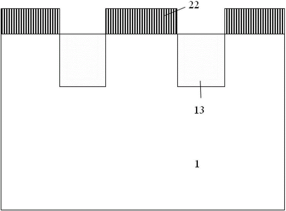
[0039] The process method for realizing the trench type IGBT of the minority carrier storage layer of the present invention comprises the steps of:

[0040] 1) On an N-type silicon wafer 1 [N-type {100} silicon wafer] with sufficient thickness as a substrate, a layer of silicon dioxide is deposited by thermal growth as the first hard mask 22 (two The thickness of silicon oxide depends on the etching depth of the etched trench. For example, for a 4μm trench, the thickness of silicon dioxide is generally greater than 3000 angstroms). The mask defines the pattern of the shallow trench, which is etched by dry or wet. opening the first hard mask 22;

[0041] Wherein, the thickness of the N-type silicon chip 1 is determined by the design withstand voltage value of the minority carrier storage layer trench IGBT device. For example, for a 1700-volt non-punch-through IGBT, the thickness of the N-type silicon chip is generally greater than 280 microns.

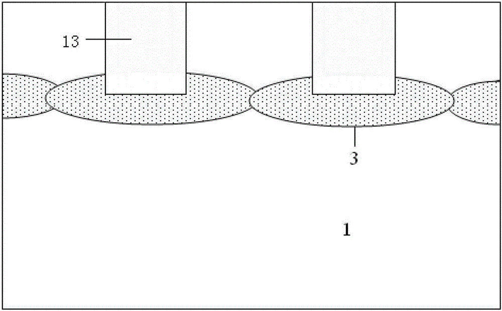
[0042] 2) Using a dry silicon e...


PUM


Abstract

The invention discloses a process method for achieving a minor carrier storage layer groove-type insulated gate bipolar translator (IGBT). The process method for achieving the minor carrier storage layer groove-type IGBT comprises the steps, (1) depositing a first hard covering film on an N type silicon wafer, defining a pattern of a shallow groove, and opening the first hard covering film in an etching mode, (2) forming the shallow groove, (3) forming an N type minor carrier storage layer, (4) removing the first hard covering film, (5) opening a second hard covering film, (6) forming a deep groove and removing the second hard covering film, (7) forming a grid electrode, (8) forming a P well region of the minor carrier storage layer IGBT, (9) forming an N + region, (10) leading out an electrode of the grid and an electrode of an emitting electrode, (11) finishing a front process of the N type silicon wafer, thinning the back of the silicon wafer, forming an FS region and a P + region on the back of the silicon wafer, evaporating metal from the back of the silicon wafer, and forming a collector electrode. According to the process method for achieving the minor carrier storage layer groove-type IGBT, the minor carrier storage layer is not formed through an epitaxial method or a high-energy injection method, minor carrier concentration of a region close to an IGBT channel is lower, and influence on IGBT threshold voltage is reduced.

Description

technical field [0001] The invention relates to an IGBT (Insulated Gate Bipolar Transistor, insulated gate bipolar transistor) process method in a power semiconductor device, in particular to a process method for realizing a minority carrier storage layer trench type IGBT. Background technique [0002] IGBT power device is a new type of power semiconductor device with rapid development and wide application. It is based on ordinary double diffused metal oxide semiconductor (DMOS), by introducing P+ structure in the collector, in addition to DMOS high input impedance, fast switching speed, high operating frequency, easy voltage control, good thermal stability, drive In addition to the characteristics of simple circuit and easy integration, the on-resistance and on-state power consumption are greatly reduced through the conductance modulation effect of collector hole injection. At present, power IGBT has been widely used in frequency conversion home appliances, wind power gene...

Claims


Application Information

Patent Timeline
Patent Type & Authority Patents(China)
IPC IPC(8): H01L21/331H01L21/265
Inventor 迟延庆
Owner SHANGHAI HUAHONG GRACE SEMICON MFG CORP
Features
  • R&D
  • Intellectual Property
  • Life Sciences
  • Materials
  • Tech Scout
  • Unparalleled Data Quality
  • Higher Quality Content
  • 60% Fewer Hallucinations
Learn More