Vapor-phase epitaxy deposition apparatus realizing nitride crystal homoepitaxy

A nitride crystal, vapor phase epitaxy technology, applied in the direction of crystal growth, chemical reactive gas, single crystal growth, etc., can solve the problems of inability to meet commercialization, difficult to achieve large-scale GaN single crystal, etc., to improve quality and growth. Speed, performance-enhancing effects

Inactive Publication Date: 2013-05-08
甘志银
View PDF5 Cites 4 Cited by
  • Summary
  • Abstract
  • Description
  • Claims
  • Application Information

AI Technical Summary

Problems solved by technology

At present, the methods for growing GaN bulk single crystal mainly include high temperature and high pressure method, sublimation method, Na melting crystallization method and hydride vapor phase epitaxy method, among which the first three methods have high requirements on equipme...

Method used


Image

  • Vapor-phase epitaxy deposition apparatus realizing nitride crystal homoepitaxy
  • Vapor-phase epitaxy deposition apparatus realizing nitride crystal homoepitaxy
  • Vapor-phase epitaxy deposition apparatus realizing nitride crystal homoepitaxy

Examples


Embodiment 1

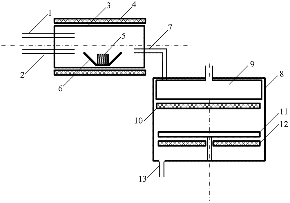
[0018] Such as figure 1 Shown is a schematic diagram of the design of the device of the present invention.

[0019] The outside of the metal chloride supply chamber 3 is provided with a heating device 4 and a ventilation pipe for introducing hydrogen chloride reaction gas or hydrogen or nitrogen as a carrier gas, and the generated metal chloride reaction gas is carried by the carrier gas into the metal organic compound vapor phase epitaxy reaction chamber; A quartz boat 6 is arranged inside the chloride supply chamber 3, and a reaction gas inlet device 9 is arranged on the upper part of the metal-organic compound vapor phase epitaxy reaction chamber 8 (abbreviation: vapor phase epitaxy reaction chamber), which can make the organic matter of gallium, indium, magnesium, and aluminum Reaction gas, group V source reaction gas such as ammonia and silane and other dopant source gases enter the reaction chamber; the lower part of the vapor phase epitaxy reaction chamber 8 is provided...

Embodiment 2

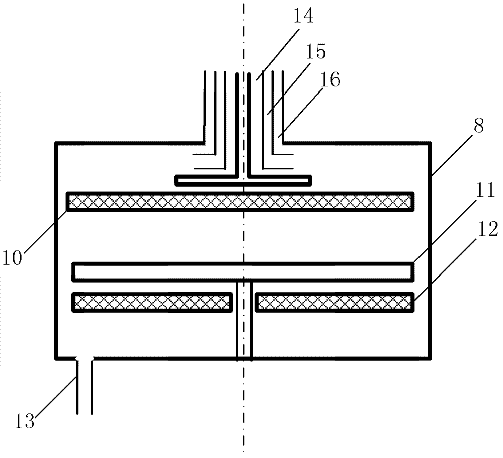
[0022] This embodiment is the same as the above-mentioned implementation one, the difference is that the reactant gas inlet device is as follows figure 2 As shown in the central three-laminar nozzle inlet structure, when the gallium nitride thick film is growing, the gallium chloride gas and the carrier gas enter the vapor phase epitaxy reaction chamber 8 through the inlet pipe 15, and the mixed gas of ammonia gas and the carrier gas It enters the reaction chamber 8 through the gas inlet pipe 14 and the gas inlet pipe 16; when growing the gallium nitride thin film, the metal gallium organic compound carried by the carrier gas is fed through the gas inlet pipe 15.

Embodiment 3

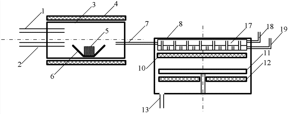
[0024] This embodiment is the same as Embodiment 1, the difference is that the reaction gas inlet device is such as image 3 In the spray structure shown, when the gallium nitride thick film is grown, the gallium chloride gas and the carrier gas enter the gas buffer chamber of the spray 17 through the intake pipe 7, and the mixed gas of ammonia gas and the carrier gas flows from the intake gas The pipeline 19 enters the gas buffer chamber of the spray 17, and the two reaction gases flow out from the spray hole and then mix and react; Gas-carried gallium metal organic compounds.


PUM


Abstract

The invention relates to a vapor-phase epitaxy deposition apparatus realizing nitride crystal homoepitaxy. The device comprises a metal chloride supply chamber and a vapor-phase epitaxy reaction chamber. A heating device and a ventilation pipe are arranged outside the supply chamber. A quartz vessel is arranged inside supply chamber for accommodating a metal source. A reaction gas feeding device is arranged on the upper part of the vapor-phase epitaxy reaction chamber. A sheet carrier palate is arranged inside the vapor-phase epitaxy reaction chamber and is used for accommodating substrate materials. Heating devices are arranged above and below the sheet carrier plate. The device provided by the invention has the advantage that the heating devices are arranged above and below the sheet carrier plate, such that temperature gradient distribution in the reaction chamber is changed. Advantages of hydride vapor-phase epitaxy and metal organics chemical vapor-phase epitaxy are composed, such that nitride hydride epitaxy and metal organics epitaxy are realized in a same reaction chamber. Therefore, thick film and thin film epitaxial growth are realized, and homoepitaxy is realized. The invention can also be used in a process for improving an independent metal organics epitaxy process through changing the temperature gradient in the reaction chamber. Therefore, nitride crystal quality can be improved, and device performance can be improved.

Description

technical field [0001] The invention belongs to the technical field of semiconductors and relates to a vapor phase epitaxial deposition device capable of realizing nitride homoepitaxial growth. Background technique [0002] Nitride materials represented by gallium nitride (GaN)-based compounds have the characteristics of energy bandwidth, high saturation electron velocity, high breakdown voltage, and small dielectric constant. For GaN, its chemical properties are stable, high temperature resistance, and corrosion resistance, and it is very suitable for making radiation-resistant, high-frequency, high-power and high-density integrated electronic devices as well as blue, green and ultraviolet optoelectronic devices, so GaN-based compound materials At present, it has become a research hotspot of rapid development. [0003] The growth methods of GaN-based semiconductor materials mainly include metal organic vapor phase epitaxy (MOCVD), hydride vapor phase epitaxy (HVPE) and mol...

Claims


Application Information

Patent Timeline
IPC IPC(8): C30B25/10C30B29/40
Inventor 甘志银
Owner 甘志银
Why Eureka
Try Eureka