Method for manufacturing multi-layer metal mobile microstructure on metal base

A multi-layer metal and metal substrate technology, applied in the electrolytic process, electroforming and other directions, can solve the problems of difficulty in making movable microstructures, easy separation, fragile substrates, etc., to achieve strong impact resistance, high microstructure strength, Good verticality of side walls

Inactive Publication Date: 2013-05-15
DALIAN UNIV OF TECH
View PDF7 Cites 8 Cited by
  • Summary
  • Abstract
  • Description
  • Claims
  • Application Information

AI Technical Summary

Problems solved by technology

[0004] The purpose of the present invention is to provide a method for manufacturing a multilayer metal movable microstructure on a metal substrate, which solves the problems of easy separation between layers of multilayer metal microstructure, fragile substrate, and difficulty in making movable microstructures

Method used


Image

  • Method for manufacturing multi-layer metal mobile microstructure on metal base
  • Method for manufacturing multi-layer metal mobile microstructure on metal base
  • Method for manufacturing multi-layer metal mobile microstructure on metal base

Examples


Embodiment Construction

[0033] The specific implementation manners of the present invention will be described in detail below in combination with the above technical solutions and accompanying drawings.

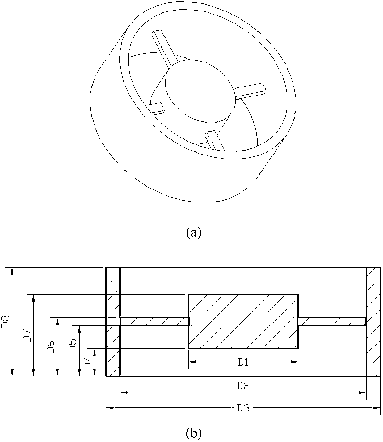
[0034] For example: to make a multi-layer metal movable microstructure on a high-purity nickel plate with a nickel content of 99.99% after fine grinding and polishing. The size of the nickel plate is 63×63×3㎜. The specific steps for making this structure are as follows:

[0035] (1) Substrate pretreatment: The substrate pretreatment is divided into two parts: mechanical processing pretreatment and surface cleaning; the substrate material is high-purity nickel plate; the surface roughness Ra value of the nickel plate substrate after machining is 0.03-0.04 μm; the surface cleaning adopts After wiping with acetone cotton ball, ultrasonically clean in acetone and ethanol for 15 minutes respectively;

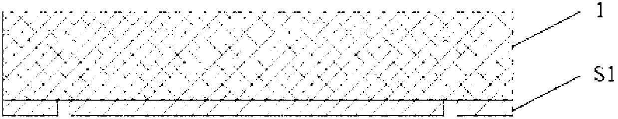
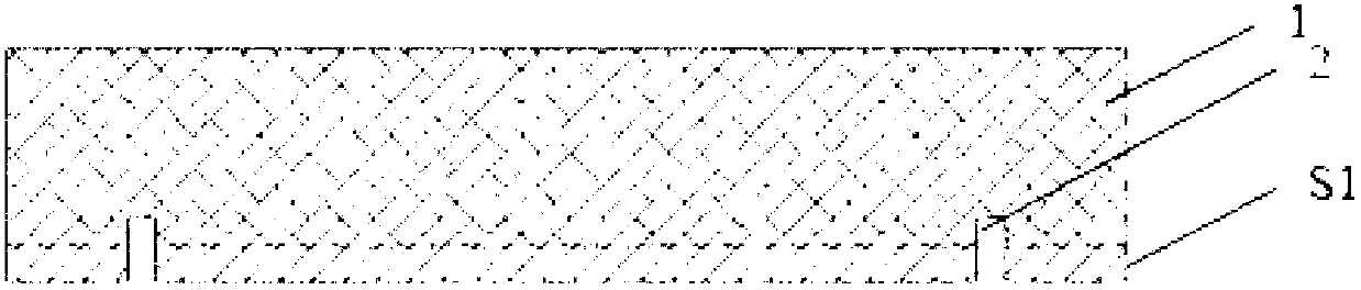
[0036] (2) Make the alignment mark on the back: perform SU-8 photoresist photolithography on the back o...


PUM

PropertyMeasurementUnit
surface roughnessaaaaaaaaaa
thicknessaaaaaaaaaa
particle sizeaaaaaaaaaa

Abstract

The invention relates to a method for a manufacturing multi-layer metal mobile microstructure on a metal base, belonging to the technical field of micro-manufacture and relating to metal base micro electroforming metal devices. The method is characterized in that the multi-layer metal mobile microstructure can be manufactured on a high-purity nickel plate base through repeated SU-8 photoresist overlay, conducting layer preparation, repeated micro electroforming nickel and micro electroforming post treatment. In the manufacture process of conducting layer, copper is selected as a conducting material; residual stress is removed by vacuum annealing in an annealing process, and the binding force between layers is improved simultaneously; and in the glue film removing process, a concentrated sulfuric acid boiling manner is adopted. The method has the beneficial effects that the prepared multi-layer metal mobile microstructure has the advantages that the layers are combined firmly, the inner stress of the microelectroforming layer is small, the microstructure has strong shock resistance, the side wall is good in verticality, the surface smoothness is high, and the like.

Description

technical field [0001] The invention belongs to the technical field of micro-manufacturing, and relates to metal substrate micro-electroforming metal devices, in particular to a method for manufacturing a multilayer metal movable microstructure on a metal substrate. Background technique [0002] With the miniaturization of devices and the development of MEMS technology, multilayer metal movable microstructures, as the core components of microsensors / actuators, have been widely used in communications, medical treatment, biology, precision instruments, aerospace, optical alignment, Integrated circuits and other fields have been applied. Its processing method has attracted more and more attention of researchers. The existing multilayer metal microstructures are mainly fabricated by sputtering seed layers on insulating substrate silicon or glass, photolithography, electroforming and other methods. For example, pages 75-78 of the first issue of "Microfabrication Technology" in ...

Claims


Application Information

Patent Timeline
Patent Type & Authority Applications(China)
IPC IPC(8): C25D1/00
Inventor 杜立群李成斌王翱岸
Owner DALIAN UNIV OF TECH
Why Eureka
Try Eureka