Novel self-assembly method of ordered Ge/Si quantum dot array by nano-pore replication and sputtering deposition

A technology of nanoholes and quantum dots, which is applied in the growth field of self-organized Ge/Si quantum dots, and can solve the problems of not being able to use low cost, not being able to reach the substrate surface, and removing by wet chemical methods

Inactive Publication Date: 2013-05-22
YUNNAN UNIV
View PDF4 Cites 14 Cited by
  • Summary
  • Abstract
  • Description
  • Claims
  • Application Information

AI Technical Summary

Problems solved by technology

Since this method uses anodized metal Al foil, it is difficult to prepare an AAO template with a thickness of less than 100 nm and a highly uniform and ordered nanopore distribution.
Due to the thick template prepared by this method, it is easy to cause "shadow effect" and "self-sealing effect" during the growth of quantum dots, resulting in atoms deposited on the surface of the template blocking the nanopores and unable to reach the substrate surface. Defects in the array
Since the distribution uniformity and order of the nanopores on the surface of the AAO template are affected by the Al foil, its long-range uniform order cannot be compared with that of the quantum dot array prepared by photolithography.
At the same time, using this method, it is necessary to peel off the AAO from the Al base, remove the barrier layer and transfer it to the semiconductor substrate. On the one hand, the binding force between AAO and the substrate is weak. On the other hand, due to the weak strength of the ultra-thin AAO template , it is very difficult to transfer it to semiconductor substrates without destroying the fragile porous structure
In addition, using this method to grow Ge / Si quantum dots, due to the corrosion effect of water on Ge quantum dots, the low-cost wet chemical method cannot be used to remove the AAO template on the substrate surface, resulting in a complicated process.

Method used


Image

  • Novel self-assembly method of ordered Ge/Si quantum dot array by nano-pore replication and sputtering deposition
  • Novel self-assembly method of ordered Ge/Si quantum dot array by nano-pore replication and sputtering deposition
  • Novel self-assembly method of ordered Ge/Si quantum dot array by nano-pore replication and sputtering deposition

Examples


Embodiment 1

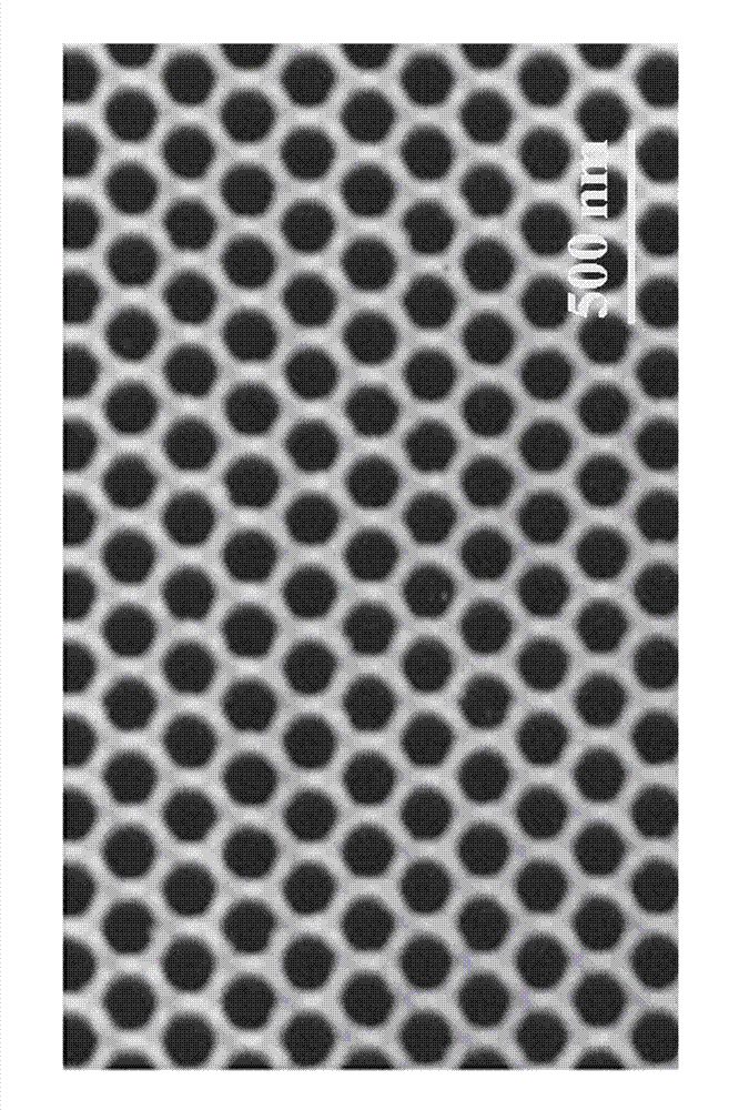
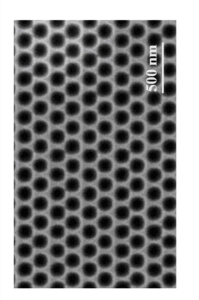
[0034] To prepare a diameter of 100 nanometers and a Ge / Si quantum dot array with a distribution period of 200 nanometers as an example to illustrate the content of the present invention:

[0035] First, the ultra-thin Si-based AAO is prepared, and the (100)-oriented n-type single crystal Si is selected as the substrate. After the substrate is cleaned by the standard Shiraki method, it is dried with high-purity nitrogen and transferred to a high-vacuum sputtering deposition chamber. The vacuum degree of the body is better than 3.0×10 -4 Pa, at a substrate temperature of 300 °C, a metal Al film with a thickness of 1.5 microns was deposited on the surface of a Si substrate by sputtering, and the Al film was pre-woven by extruding the Al film with a quartz template with nanopillars periodically distributed on the surface. Texturization, forming indentations with a diameter and period of 100 nanometers and a period of 200 nanometers, and a depth of 20 nanometers on the surface of ...


PUM

PropertyMeasurementUnit
thicknessaaaaaaaaaa
thicknessaaaaaaaaaa
diameteraaaaaaaaaa

Abstract

The invention provides a method of self-assembly growth of a large-area, even and ordered Ge quantum dot array on a Si substrate by sputtering deposition. The method includes preparation of ultrathin Si-based AAO (anodic aluminum oxide), preparation of a pattern substrate by nano-pore replication, and self-assembly growth of the even, ordered Ge quantum dot array on the surface of the pattern substrate by ion beam sputtering. Quantum dot growth process matching with the pattern substrate is obtained by controlling ion beam sputtering deposition temperature, ion beam flux voltage, and buffer layer thickness, so that Ge quantum dot nano-pores evenly and orderly grow at nucleation center. Even-size Ge quantum dots obtained are in hexagonal symmetrical distribution on the surface of the Si substrate, and the diameter of the quantum dots is adjustable. The method effectively overcomes the defects that distribution of the self-assembled Ge/Si quantum dots is random and disorder in position, the size is uneven, controllability is low, and preparation cost is high. The large-area, even, ordered and small-sized Ge quantum dot array is prepared at low cost. The method is applicable to manufacture of devices such as silicon-base quantum-dot light emitters, quantum-dot photoelectric detectors and efficient quantum-dot solar cells.

Description

technical field [0001] The invention relates to a large-area, highly uniform and ordered self-organized Ge / Si quantum dot growth technology, which belongs to the technical field of preparation and application of nanometer materials and structures. Background technique [0002] Since Si is the chip material of large-scale integrated circuits, new photoelectric functional devices hope to realize the integration of light-emitting devices, photodetection devices, energy conversion devices and existing microelectronic devices on the same Si chip. However, the indirect band gap of Si leads to extremely low luminous efficiency, and the band gap of Si at room temperature is 1.12 electron volts, making it difficult to achieve photoelectric response in the mid-to-far infrared band. Quantum dots have a three-dimensional confinement effect on carriers. Therefore, by controlling the structure, size and distribution of quantum dots, the energy band structure of the material can be adjuste...

Claims


Application Information

Patent Timeline
Patent Type & Authority Applications(China)
IPC IPC(8): H01L21/203
Inventor 熊飞杨培志陈雨璐李学铭
Owner YUNNAN UNIV
Why Eureka
Try Eureka