Organic electroluminescence device and method for preparing same

An electroluminescent device and luminescent technology, which is applied in the manufacture of organic semiconductor devices, electric solid devices, semiconductor/solid device, etc., can solve the problems of large investment in hardware equipment, device performance degradation, high energy consumption, etc., and achieve investment and Low performance requirements, good device performance, and the effect of saving production costs

Inactive Publication Date: 2013-07-03
BOE TECH GRP CO LTD
View PDF2 Cites 52 Cited by
  • Summary
  • Abstract
  • Description
  • Claims
  • Application Information

AI Technical Summary

Problems solved by technology

[0007] (1) For the mixed pixel partition wall system composed of inorganic and organic components in the first method, the preparation methods and processes of the two-layer films are usually quite different, and the corresponding hardware equipment is also completely different, so the input requirements for hardware equipment Larger, thus resulting in higher actual production costs
[0008] (2) In addition, the adhesion between the inorganic layer and the organic layer is generally weak, and it is easier to separate the inorganic layer and the organic layer when subjected to external force or bending, resulting in a decrease in device performance
[0009] (3) For thin films of inorganic materials, chemical vapor deposition, physical vapor deposition, atomic layer deposition or evaporation are often used to prepare them. The production process requires special reactive gases (usually toxic gases) and high energy consumption. etc. At the same time, these processes are generally carried out under a certain degree of vacuum, and the investment and performance requirements for equipment are relatively high.

Method used


Image

  • Organic electroluminescence device and method for preparing same
  • Organic electroluminescence device and method for preparing same
  • Organic electroluminescence device and method for preparing same

Examples


preparation example Construction

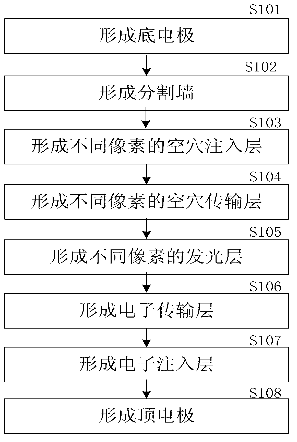
[0064] The method for preparing an organic electroluminescent device of the present invention comprises the steps of:

[0065] Step 1, depositing and patterning a bottom electrode on the substrate containing the driving transistor;

[0066] Step 2. Prepare a multi-layer pixel partition wall by coating on the above-mentioned substrate deposited with the patterned bottom electrode, and the pixel partition wall includes a lyophilic organic material separation layer and a lyophobic organic material separation layer;

[0067] Step 3, depositing and preparing a functional layer on the pixel area defined by the partition wall;

[0068] Step 4, sequentially depositing a cathode, a protection layer or an encapsulation layer on the functional layer and the pixel separation wall.

[0069] The method for preparing an organic electroluminescent device of the present invention, wherein, comprises the following steps:

[0070] Step 1. Prepare the bottom layer of the partition wall by coati...

Embodiment 1

[0078] Example 1. Organic electroluminescent device with double-layer pixel partition walls

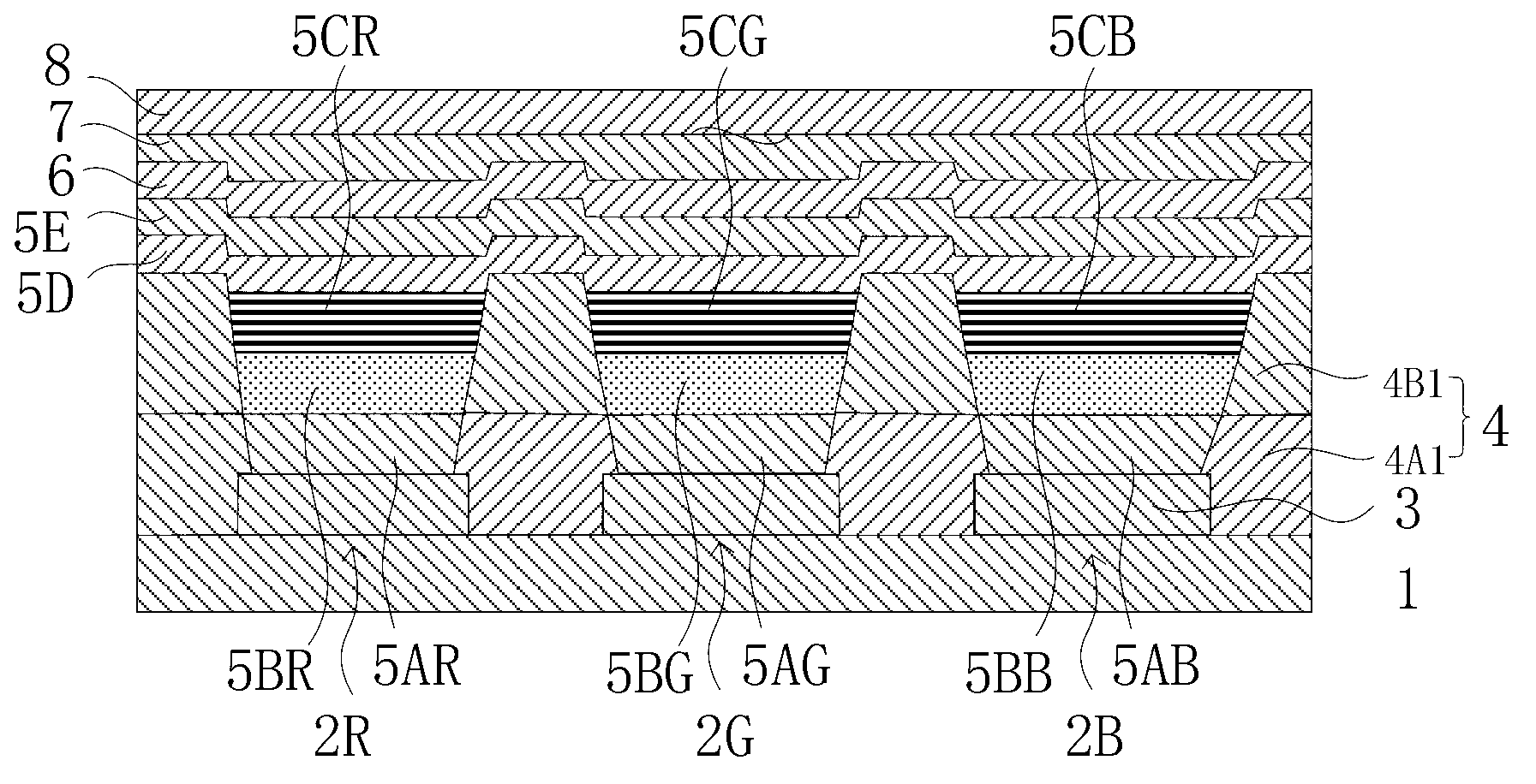
[0079] figure 1 A cross-sectional view of one example of the organic electroluminescence device of the present invention is shown. The organic electroluminescent device is composed of the following parts: substrate 1 (carrying light-emitting units 2R, 2G, 2B), bottom electrode 3 (anode referred to in this embodiment) deposited sequentially on the substrate, and pixel separation wall 4 (first separation layer 4A1 and second separation layer 4B1), hole injection layer 5A, hole transport layer 5B, light emitting layer 5C, electron transport layer 5D, electron injection layer 5E, top electrode 6 as a cathode, protective layer 7 and package substrate 8 .

[0080] The substrate 1 mainly carries the red organic electroluminescent unit 2R, the green organic electroluminescent unit 2G and the blue organic electroluminescent unit 2B thereon. The substrate material of the substrate may be qua...

Embodiment 2

[0093] Example 2. Organic electroluminescent device with multi-layered pixel partition walls

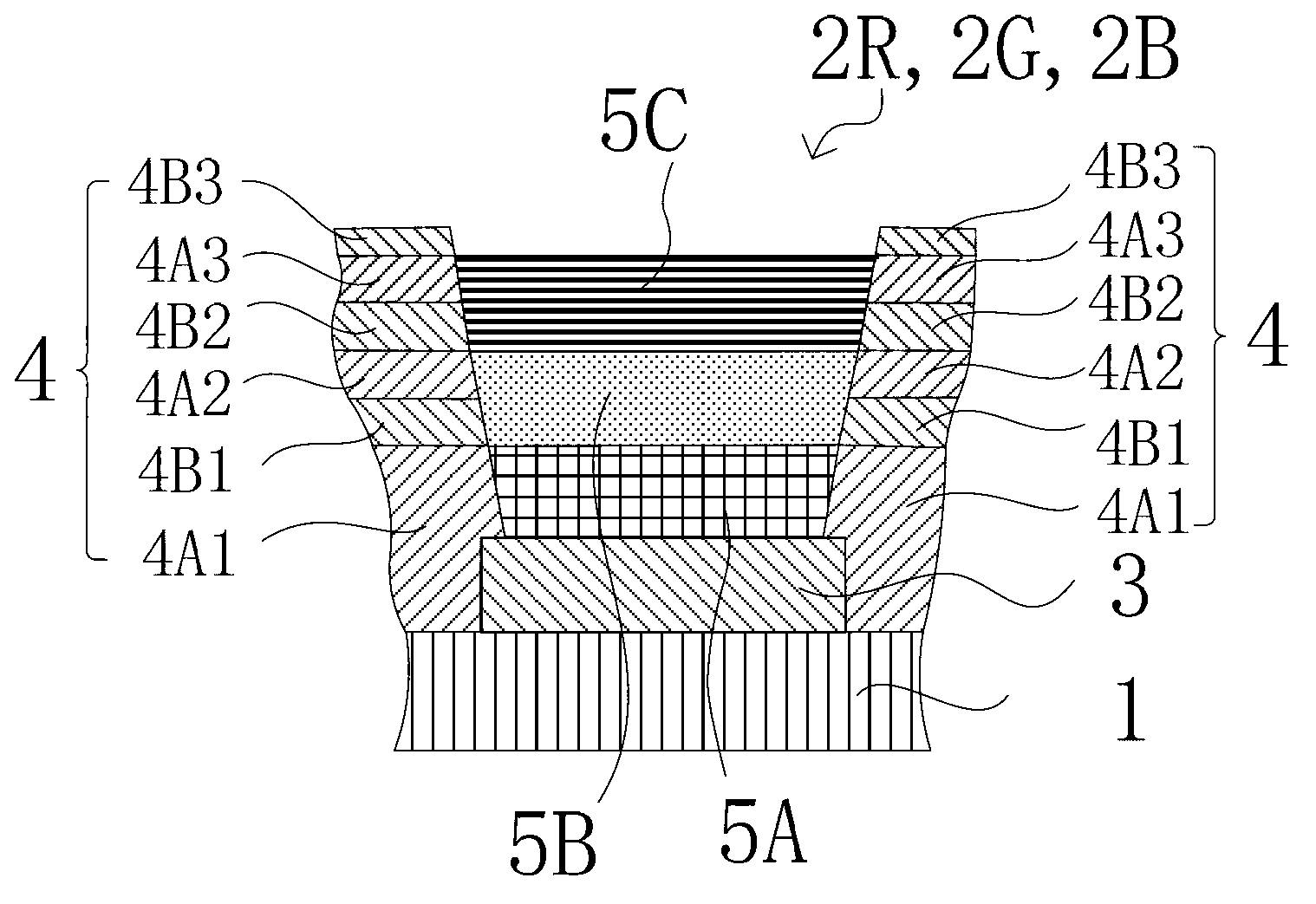
[0094] figure 2 A schematic diagram of an organic electroluminescence device having a multilayered pixel partition wall as the present embodiment is shown. The organic electroluminescent device in this embodiment is the same as the organic electroluminescent device in the first embodiment, the difference is that the pixel partition wall 4 is composed of more than two (multiple) separation layers stacked, each separation layer Using organic materials, the wettability of adjacent separation layers is different, the same components are designated with the same reference numerals, the details of which are not described again.

[0095] In the multi-layer pixel partition wall structure shown in this embodiment, each layer ( 4A1 , 4B1 , 4A2 , 4B2 , 4A3 and 4B3 ) constituting the pixel partition wall is composed of organic materials, such as polymer materials. The wettability of adjacent ...


PUM


Abstract

The invention provides an organic electroluminescence device and a method for preparing the same. The organic electroluminescence device comprises a baseplate, wherein the baseplate is provided with pixel separation walls, the pixel separation walls are composed of at least two organic material isolating layers in a stacking manner, and the wetting properties of the adjacent organic material isolating layers are different. The method for preparing the organic electroluminescence device provided by the invention comprises the following steps of: depositing a bottom electrode and a pattern, preparing two layers or multiple layers of the pixel separation walls; and depositing and preparing a functional layer, and sequentially depositing a cathode, a protective layer or a packaging layer. According to the organic electroluminescence device provided by the invention, the pixel separation walls are composed of at least two organic material isolating layers in a stacking manner, and the wetting properties of adjacent organic material isolating layers are different, the bonding force of the isolate layers in layer upon layer of organic materials is generally stronger, and the property of a device is good. The method for preparing the organic electroluminescence device provided by the invention has the advantages that the steps are simple, and therefore, the manufacturing cost is saved.

Description

technical field [0001] The invention relates to the field of electroluminescence, in particular to an organic electroluminescence device and a method for preparing the organic electroluminescence device. Background technique [0002] In recent years, as a new type of flat panel display, organic electroluminescence display has received more and more attention. Organic electroluminescent displays are characterized by thinness, wide viewing angle, low power consumption, fast response speed, and flexible display. Since it is an active light-emitting device, it is considered to have a great advantage in displaying high-definition high-speed video, and it is developing toward practicality in recent years. The core component of an organic electroluminescent display is an organic electroluminescent device. [0003] Forming the light-emitting layer of an organic electroluminescent device (OLED), etc., can generally be divided into small molecule materials and high molecule (polymer...

Claims


Application Information

Patent Timeline
Patent Type & Authority Applications(China)
IPC IPC(8): H01L27/32H01L51/52H01L21/77
CPCH10K59/35H10K59/122H10K71/13H10K2102/351H10K50/11H10K71/00H10K71/10H10K71/231
Inventor 代青刘则孙力
Owner BOE TECH GRP CO LTD
Why Eureka
Try Eureka