
Refining method for alkaline treatment fluid for semiconductor substrate and refining device

The technology of a substrate processing device and a refining method, which is applied in the fields of semiconductor/solid-state device manufacturing, semiconductor device, adsorbed water/sewage treatment, etc., can solve the problems of Fe pollution, economic difficulty, removal of Fe pollution, etc., and achieve excellent chemical resistance. Quality and mechanical strength, high refining effect, easy preparation effect

Inactive Publication Date: 2013-07-03
TAMA KAGAKU IND +1
View PDF9 Cites 5 Cited by
  • Summary
  • Abstract
  • Description
  • Claims
  • Application Information

AI Technical Summary

Problems solved by technology

Therefore, further adsorption purification cannot be performed
Silicon particles with an Fe concentration of 0.1ppm or less can be produced by the CVD fluidized bed method, but it is difficult from an economic point of view
In addition, even if silicon ingots for semiconductors are pulverized to produce silicon particles, Fe contamination will occur from the pulverizer, and it is difficult to remove the Fe contamination by washing, etc. In this method, even if the Fe concentration is 0.1ppm

Method used


Image

  • Refining method for alkaline treatment fluid for semiconductor substrate and refining device
  • Refining method for alkaline treatment fluid for semiconductor substrate and refining device
  • Refining method for alkaline treatment fluid for semiconductor substrate and refining device

Examples


Embodiment 1

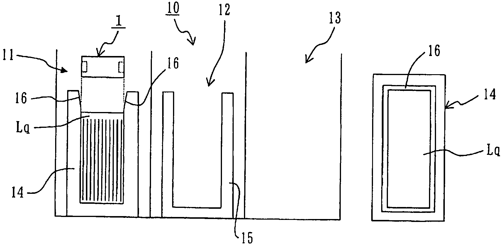
[0101] Using two silicon carbide single crystal (6H) wafers with a diameter of 75 mm, the atomic force microscope (AFM) images of the mirror surfaces of these wafers were obtained in advance, and the mirror surfaces were arranged to face each other. As in the case of the previous Fe adsorption purification experiment, the formation of The adsorption sheet laminate of Example 1 with slits at a gap of 0.5 mm.

[0102] To the adsorption plate laminate of Example 1, radioactivity was added to the above-mentioned 5wt%-choline aqueous solution 59 Radioactivity from Fe 59 For the test solution with an Fe concentration of 100ppt, the Fe adsorption and purification experiment was carried out at room temperature in the same procedure as in the previous Fe adsorption and purification experiment, and the radioactivity of the test solution was obtained. 59 The residual rate of Fe.

[0103] Then, after washing the inside of the slit of the adsorption plate laminate in Example 1 in the sam...

Embodiment 2

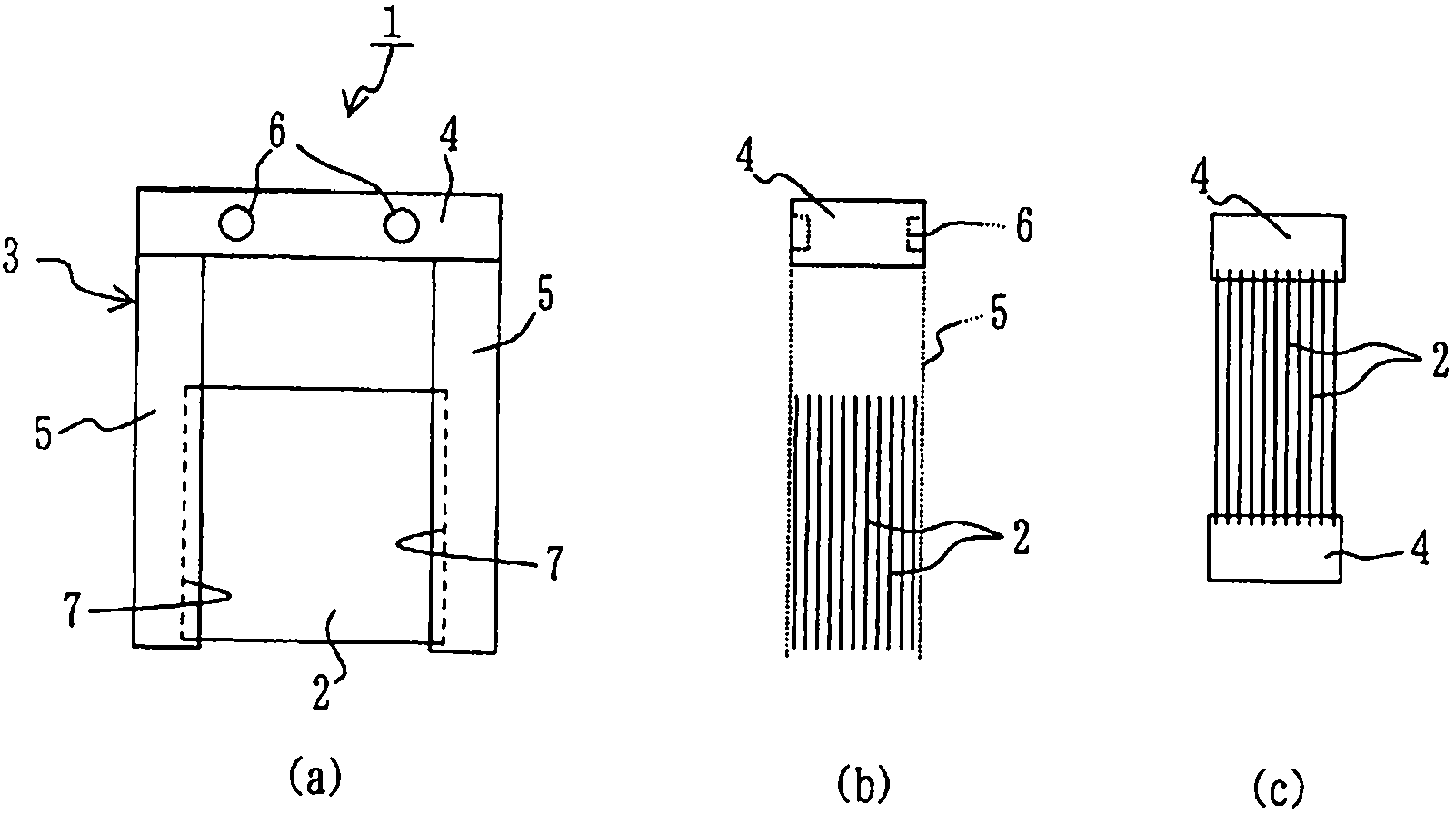
[0110] Based on the findings of the above-mentioned Example 1, as an adsorption purification device for alkaline treatment liquid, a figure 1 (a) ~ figure 1 The adsorption sheet laminate 1 shown in (c). The adsorption plate laminate 1 is cut out from a 0.6mm thick CVD polycrystalline pseudowafer (K≒0.3, with good hydrophilicity on both the surface and the back surface) by laser processing, in the form of a set of 11 pieces of 100mm×102mm in size. The adsorption plates 2 and the holding boxes 3 made of fluororesin (PTFE) hold these adsorption plates 2 at a predetermined interval (usually 0.8 to 3.0 mm, preferably 1 to 2 mm) in parallel and facing each other. . Furthermore, the holding box 3 is composed of a box top 4 having a concave portion 6 for connecting to a robot arm (not shown) for conveyance and positioning of the adsorption sheet laminate 1 and hanging from both ends of the box top 4 and facing each other. The inner surface side of the box is composed of a pair of...

Embodiment 3

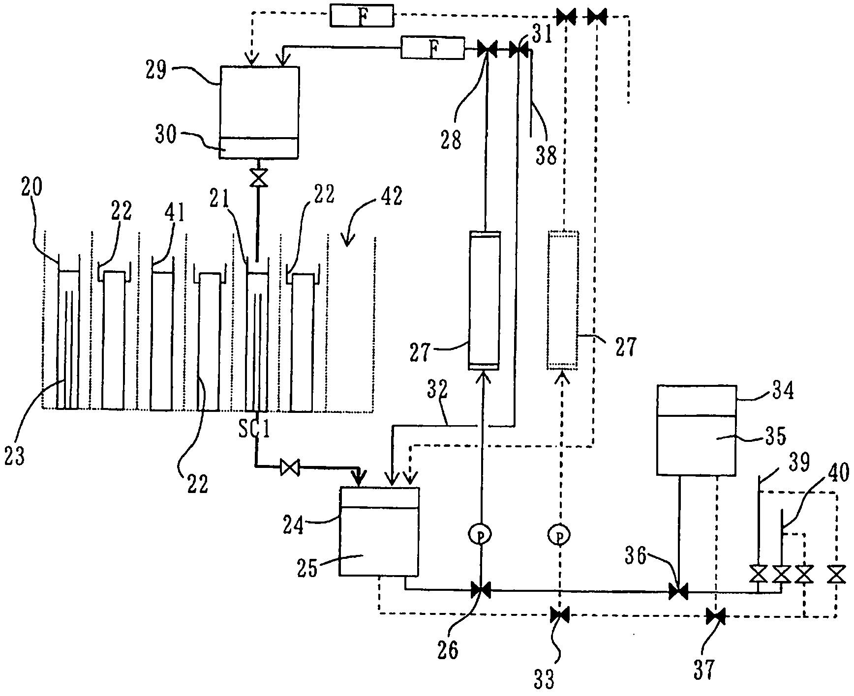
[0123] In order to use high-purity silicon carbide particles (GNF-CVD manufactured by Pacific Rundom Co., Ltd.) with a particle size of 0.2 to 1.2 mm as a single crystal raw material as an adsorption refining agent, choline stock solution and nitric acid were soaked and pre-washed separately for several days Then, 60 g (apparent volume: about 30 mL) was filled into a column made of fluororesin with an inner diameter of 20 mm and a length of about 120 mm to constitute an adsorbent packed column. First, pass each 500mL of the following liquids into the tower successively: 7wt%-nitric acid aqueous solution, ultrapure water, 2wt%-hydrofluoric acid, 1wt%-hydrogen peroxide aqueous solution, ultrapure water, and then carry out the refining of the test solution experiment.

[0124] In addition, as the alkaline treatment liquid (refined liquid), use 4wt%-choline aqueous solution (choline stock solution), this liquid to be refined of 500mL is passed in the above-mentioned adsorbent pack...


PUM

PropertyMeasurementUnit
particle diameteraaaaaaaaaa

Abstract

A method for refining alkaline treatment fluid for semiconductor substrates and a refining device are provided that are capable of refining all kinds of alkaline treatment fluid used for treating semiconductor substrates for a variety of purposes, to an ultrahigh purity, particularly Fe concentrations to ppq levels, and which use an absorbing and purifying means with excellent chemical resistance and mechanical strength. Specifically provided are a refining device and a method for refining alkaline treatment fluid for semiconductor substrates, which are means for refining alkaline treatment fluid for treating semiconductor substrates for a variety of purposes when producing semiconductor substrates or semiconductor devices, and whereby alkaline treatment fluid is brought in contact with a silicon carbide crystal surface of an absorbing and purifying means and made to flow into gaps in, for example, an absorption plate laminate (2) wherein both surfaces are CVD silicon carbide surfaces, and metal impurities are made to attach to the silicon carbide crystal surface and removed.

Description

technical field [0001] The present invention relates to a purification method and a purification apparatus for an alkaline treatment liquid used for various purposes in the manufacture of a semiconductor substrate or in the manufacture of a semiconductor device using the semiconductor substrate, etc., and more specifically Specifically, the present invention relates to a method for refining an alkaline treatment solution for semiconductor substrates and a refining device for carrying out the method. The method for refining can contain a very small amount of various substances used in processing these semiconductor substrates as needed. The area where metal impurities, especially iron (Fe), which pollute the surface of the semiconductor substrate and are harmful to devices manufactured from the semiconductor substrate, are reduced to ppq (one-thousandth of ppt) in the alkaline treatment solution. Background technique [0002] For example, as a typical alkaline treatment solut...

Claims


Application Information

Patent Timeline
Patent Type & Authority Applications(China)
IPC IPC(8): H01L21/304B01J20/10C02F1/28C02F1/42
CPCB01J20/0251B01J20/28035H01L21/02052H01L29/1608B01J20/10C02F1/28H01L21/302
Inventor 村冈久志长俊连
Owner TAMA KAGAKU IND
Learn More