LED photonic crystal containing left-handed material and preparation method

A technology of left-handed materials and photonic crystals, applied in semiconductor devices, electrical components, circuits, etc., can solve problems that do not involve applications, achieve the effects of simplifying process steps, improving the quality of epitaxial structures, and reducing defect density

Active Publication Date: 2013-07-31
XI AN JIAOTONG UNIV
View PDF5 Cites 4 Cited by
  • Summary
  • Abstract
  • Description
  • Claims
  • Application Information

AI Technical Summary

Problems solved by technology

The previous patents involved the preparation process of left-handed materials, and did not involve the structural des

Method used


Image

  • LED photonic crystal containing left-handed material and preparation method
  • LED photonic crystal containing left-handed material and preparation method
  • LED photonic crystal containing left-handed material and preparation method

Examples


Embodiment Construction

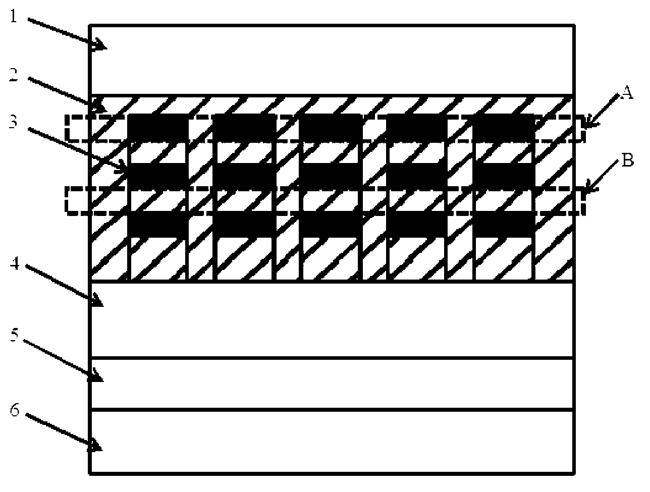
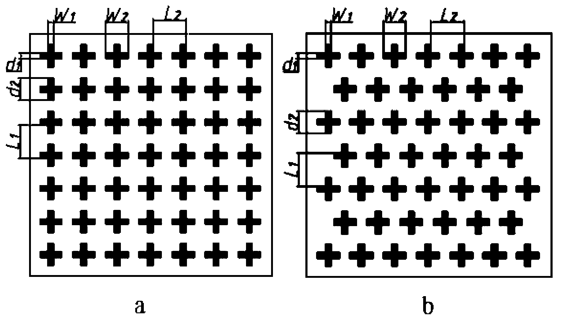
[0039] see figure 1 figure 2 , a LED photonic crystal containing left-handed materials, characterized in that, from top to bottom, it includes an n-GaN layer 1, a conductive metal substrate 2, a multi-quantum well active layer 4, a p-GaN layer 5, and a bonding metal layer 6. Among them, there is a quantum barrier GaN between the conductive metal substrate and the multi-quantum well active layer; the lower surface of the conductive metal substrate is etched upward with a "Swiss cross" void array with a depth greater than 100nm, and the plane of the "Swiss cross" void array is Upper rectangular distribution or triangular distribution, each cross gap is alternately filled with weakly conductive material 3 and conductive metal material homogeneous to the conductive metal base, each layer of weakly conductive material forms a left-hand material area A on the plane; each layer of conductive metal material The right-hand material area B on the plane is formed, and the left-hand mat...


PUM

PropertyMeasurementUnit
Depthaaaaaaaaaa
Thicknessaaaaaaaaaa

Abstract

The invention relates to an LED (light emitting diode) photonic crystal containing a left-handed material and a preparation method. The LED photonic crystal is characterized in that (1), the photonic crystal is formed by arraying a right-handed material and the left-handed material alternately; (2), gaps in a left-handed material layer are in Swiss cross structures, can be arrayed rectangularly or triangularly, and are filled with weak conducting materials; (3), a substrate of the photonic crystal is made of conducting metal; and (4), the thickness of a quantum barrier GaN between the photonic crystal and an active layer is less than 40nm. According to the LED photonic crystal and the preparation method, the LED photonic crystal is prepared by combining higher-accuracy technologies such as electron beam etching, electron beam evaporation, PECVD (plasma enhanced chemical vapor deposition), and dry etching, so that a surface plasmon enhancement effect can be generated to couple out an evanescent wave in the active layer, and wider photonic band gaps can be generated; the luminous wavelength and a light emitting angle are controlled better; and the luminous efficiency and the light emitting power of an LED are improved and increased.

Description

technical field [0001] The invention relates to a preparation technology of an optoelectronic device, in particular to a structure and a preparation method of an LED epitaxial chip. Background technique [0002] As the fourth-generation electric light source, high-power semiconductor light-emitting diode (Light Emitting Diode, hereinafter referred to as LED) has excellent characteristics such as small size, safe low voltage, long life, high light conversion efficiency, fast response speed, energy saving, and environmental protection, so it is called For "green lighting source". It is expected to replace traditional incandescent lamps and fluorescent lamps and become a new generation of light sources in the 21st century, which has great economic and social significance. At present, the application range of high-power LED is not wide, and its low luminous efficiency and low luminous flux are one of the main reasons. Vertical structure LED (Vertical Light Emitting Diode, here...

Claims


Application Information

Patent Timeline
IPC IPC(8): H01L33/06H01L33/26H01L33/00
Inventor 云峰赵宇坤
Owner XI AN JIAOTONG UNIV
Why Eureka
Try Eureka