DNA biosensor and preparation method thereof

A biosensor, sensor technology, applied in semiconductor/solid-state device manufacturing, instruments, scientific instruments, etc., can solve the problems that affect the wide application of biosensors, reduce sensor sensitivity, low hybridization efficiency, etc., achieve good electrical performance parameters, shorten detection time time, the effect of improving sensitivity

Inactive Publication Date: 2013-08-07
SHANGHAI UNIV
View PDF2 Cites 10 Cited by
  • Summary
  • Abstract
  • Description
  • Claims
  • Application Information

AI Technical Summary

Problems solved by technology

Because the realization of these two processes is time-consuming, the immobilization of DNA probes and the hybridization efficiency of DNA probes and DNA to be tested are not high, which objectively reduces the sensitivity of the sensor and affects the wide application of biosensors.

Method used


Image

  • DNA biosensor and preparation method thereof
  • DNA biosensor and preparation method thereof
  • DNA biosensor and preparation method thereof

Examples


Embodiment 1

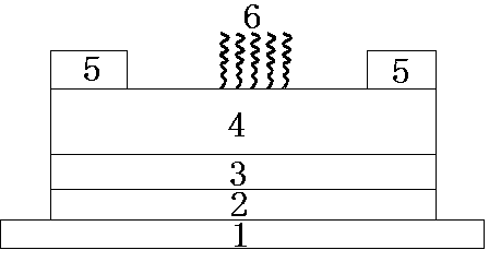
[0035] In this example, see figure 1 , a DNA biosensor, composed of an organic thin film transistor and a DNA molecular probe 6, the DNA molecular probe 6 is used as a recognition element, and the organic thin film transistor is used as a sensor transducer to convert the biological signal detected by the DNA molecular probe 6 into Easy-to-detect electrical signals. The organic thin film transistor is composed of a substrate (1), a gate electrode (2), an insulating layer (3), an organic semiconductor layer (4) and a source-drain electrode (5). The bottom (1) has a gate electrode (2) and an insulating layer (3) in sequence, and the organic semiconductor layer (4) is a P-type organic semiconductor material or an N-type organic semiconductor material; on the insulating layer (3) there is an organic semiconductor layer ( 4) Form the active layer, and then make two source-drain electrodes (5) on the organic semiconductor layer (4) to form a bottom-gate-top contact structure; apply a...

Embodiment 2

[0049] This embodiment is basically the same as Embodiment 1, especially in that:

[0050] In this example, see Figure 4 , making two source-drain electrodes 5 on the insulating layer 3, and then making an organic semiconductor layer 4 on the insulating layer 3 in the channel region between the two source-drain electrodes 5 and between the two source-drain electrodes 5 to form a carrier injection layer , forming a bottom gate bottom contact structure. In this example, a structure similar to that of Example 1 was adopted to prepare a DNA biosensor with the same function. Wherein the substrate 1 , the gate electrode 2 and the insulating layer 3 are prepared using the materials related to the first embodiment. The preparation process of insulating layer 3 is to remove heat and oxidize a layer of SiO 2 In addition, magnetron sputtering can also be used to deposit a layer of N on the silicon substrate substrate 1 2 o 5 、TiO 2 , AlN 3 、Si 3 N 4 、 Ta 2 o 5 And other relat...

Embodiment 3

[0056] This embodiment is basically the same as Embodiment 1, especially in that:

[0057] In this example, see Figure 5 , there are two layers of organic semiconductor layers 4 on the insulating layer 3 to form a double-layer active layer, that is, on the organic semiconductor layer 4, continue to make the organic semiconductor layer 4 of the second layer, and then on the organic semiconductor layer 4 of the second layer Two source-drain electrodes 5 are fabricated to form a bottom-gate-top contact structure, and DNA molecular probes 6 are fixed on the upper surface of the second organic semiconductor layer 4 . Specifically: In this embodiment, see Figure 5 Compared with the first embodiment, this embodiment is special in that: the P-type semiconductor material of the organic semiconductor layer 4 is composed of two materials of pentacene (pentacene) and copper phthalocyanine (CuPc), and two organic semiconductor layers 4 are constructed. A two-layer active layer is forme...


PUM


Abstract

The present invention discloses a DNA biosensor, which comprises an organic thin film transistor and a DNA molecule probe, wherein the DNA molecule probe is adopted as a recognition component, the organic thin film transistor is adopted as a sensor transducer for converting a biological signal detected by the DNA molecule probe into an easily detected electric signal, the organic thin film transistor comprises a base plate substrate, a gate electrode, an insulating layer, organic semiconductor layers and source drain electrodes, and the organic semiconductor layer forms an active layer or a carrier injection layer, such that the DNA molecule probe is fixed on the upper surface of the organic semiconductor layer through a physical absorption method and applying a bias voltage on the gate electrode. The present invention further discloses a DNA biosensor preparation method. According to the present invention, bias voltage applying is adopted to effectively improve DNA probe fixation and a hybridization efficiency of the DNA probe and DNA to be detected so as to increase sensor sensitivity; and compared with the conventional biosensor, the biosensor of the present invention has the following characteristics that: the same functions are achieved while a detection time is shortened.

Description

technical field [0001] The invention relates to a sensor and a manufacturing method thereof, in particular to an electrochemical biosensor combined with a semiconductor electronic device and a biological probe and a manufacturing method thereof, which is applied in the technical field of detection and monitoring device manufacturing. Background technique [0002] DNA biosensor is a high-tech product integrating modern biotechnology and advanced optoelectronic technology. It can convert non-electrical biological signals into easily observable electrical or optical signals. It has been deeply valued and widely used in fermentation technology, environmental testing, food engineering, clinical medicine, military and military medicine, etc. It is an indispensable advanced detection and monitoring device for the development of biotechnology. Due to its outstanding advantages such as high selectivity and high sensitivity, DNA sensors have shown very broad application prospects in t...

Claims


Application Information

Patent Timeline
IPC IPC(8): G01N27/414H01L51/05
Inventor 王军朱宗鹏刘娜胡玉磊桂海洋
Owner SHANGHAI UNIV
Why Eureka
Try Eureka